Tied High
Tied Low
Pass to J7
Vin1
PCM186x
(Slave)
Vin2
Vin3 Vin4
PCM9211
USB-I2X
(Master)
USB
I2C
SCKI
MCLK
BCK LRCK D
in
D
in
D
out
D
out
BCK
LRCK
www.ti.com
Hardware
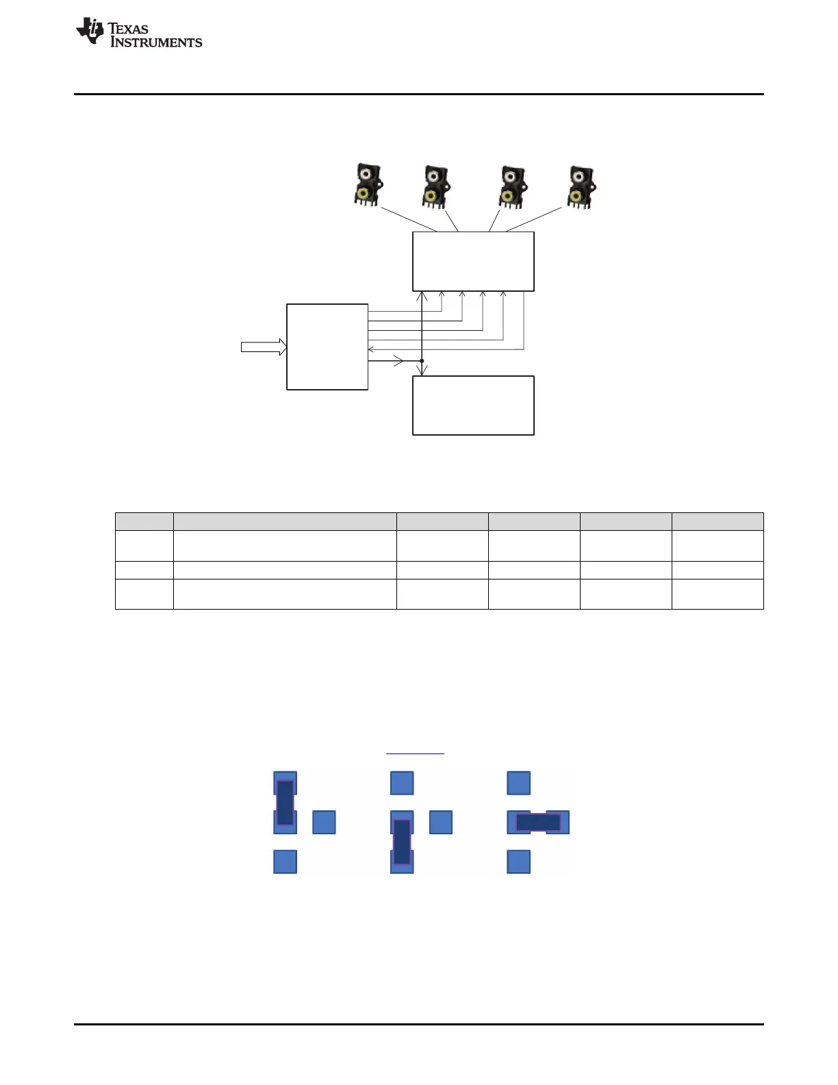
In Mode 2, the I2X board is the master (Figure 8). I2S in and out to the PCM186x is via the I2X board and
is available to a PC via USB. The optical input and output are not available. Remove Y0 and place
jumpers on J8 and J11 to use this mode.
Figure 8. Mode 2 Block Diagram
Table 3. Mode Summary
Mode Function J8 J10 J11 Crystal Y0
Mode 0 I2S input and output to PCM9211, running Installed Removed Installed Do not care
on I2S clocks
Mode1 I2S output to PCM9211 running on crystal Installed Installed Removed Installed
Mode2 I2S input and output to USB running on I2S Installed Removed Installed Do not care
clocks
4.4 Solder Options
The PCM1861 is completely hardware controlled. In addition to the hardware controlled versions of the
PCM186x family, all of the devices have GPIO. In order to accommodate these hardware and GPIO
options, a series of 3-way resistor connections are included on the EVM. Just to the left of J7, there are 8
zero-Ω resistors. By default, they are connected to pass the signals to J7. These resistors can also be
reoriented up to tie these pins high, or down to tie these pins low. For the proper settings of these multi-
function pins, see the PCM186x data sheet (SLAS831).
Figure 9. Solder Options
9
SLAU615–December 2014 PCM186xEVM
Submit Documentation Feedback
Copyright © 2014, Texas Instruments Incorporated