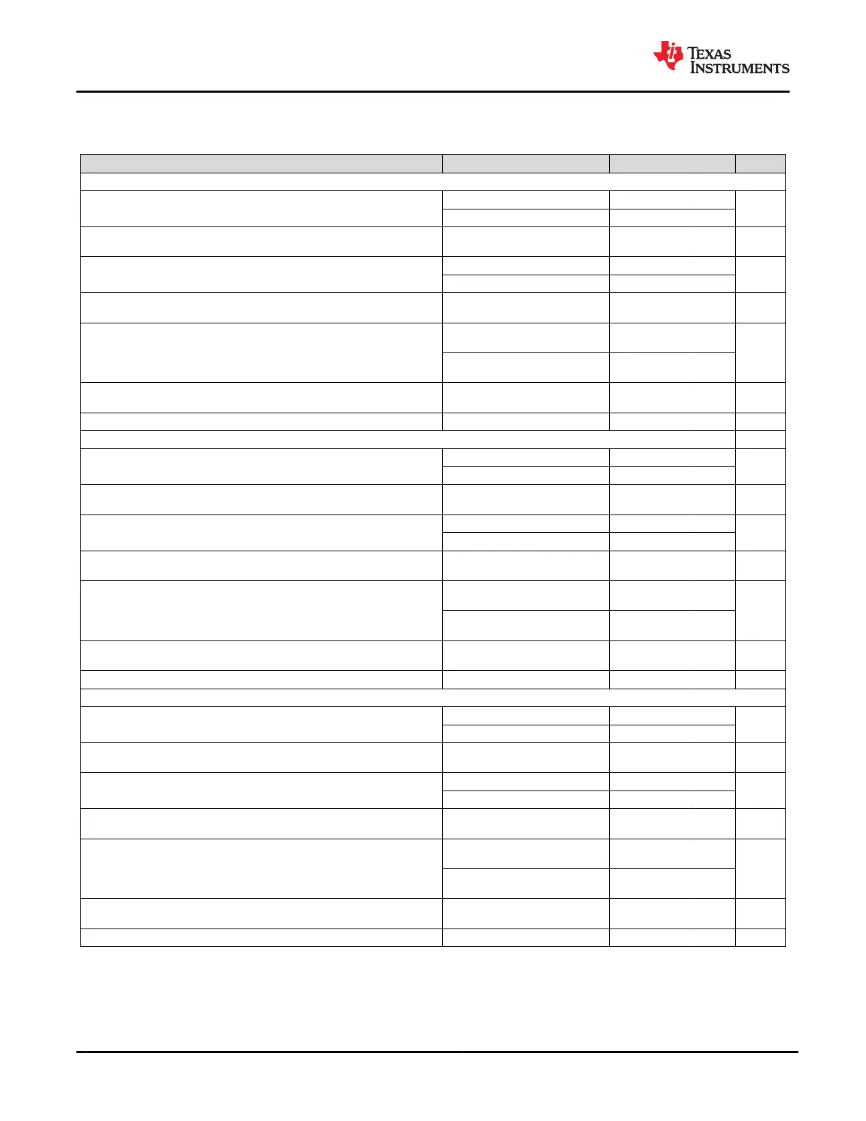
7.12 Port Data Multiplexer Switching Characteristics
Recommended operating conditions; T
A
= –10 to 85°C unless otherwise noted
PARAMETER TEST CONDITIONS MIN TYP MAX UNIT
SWD MULTIPLEXER PATH
(1)
SWD_RON_U
On resistance of SWD_DATA/CLK to
C_USB_TP/TN/BP/BN
V
i
= 3.3 V, I
O
= 20 mA 35 55
Ω
V
i
= 1 V, I
O
= 20 mA 30 46
SWD_ROND_U
On resistance difference between P and N paths of
SWD_DATA/CLK to C_USB_ TP/TN/BP/BN
V
i
= 1 V to 3.3 V, I
O
= 20 mA –2.5 2.5 Ω
SWD_RON_S On resistance of SWD_DATA/CLK to C_SBU1/2
V
i
= 3.3 V, I
O
= 20 mA 26 42
Ω
V
i
= = 1 V, I
O
= 20 mA 24 37
SWD_ROND_S
On resistance difference between P and N paths of
SWD_DATA/CLK to C_SBU1/2
V
i
= 1V to 3.3 V, I
O
= 20 mA –1.5 1.5 Ω
SWD_TON Switch on time from enable of SWD path
Time from enable bit with charge
pump off
150
μs
Time from enable bit at charge
pump steady state
10
SWD_TOFF Switch off time from disable of SWD path
Time from disable bit at charge
pump steady state
500 ns
SWD_BW 3 dB bandwidth of SWD path C
L
= 10 pF 200 MHz
DEBUG1/2 MULTIPLEXER PATH
(1)
DB1_RON_U On resistance DEBUG1/2 to C_USB_TP/TN/BP/BN
V
i
= 3.3 V, I
O
= 20 mA 14 26
Ω
V
i
= 1 V, I
O
= 20 mA 10 17
DB1_ROND_U
On resistance difference between P and N paths of
DEBUG1/2 to C_USB_TP/TN/BP/BN
V
i
= 1 V to 3.3 V, I
O
= 20 mA –2.5 2.5 Ω
DB1_RON_S On resistance of DEBUG1/2 to C_SBU1/2
V
i
= 3.3 V, I
O
= 20 mA 9.5 17
Ω
V
i
= 1 V, I
O
= 20 mA 6.5 12
DB1_ROND_S
On resistance difference between P and N paths of Debug
path DEBUG1/2 to C_SBU1/2
V
i
= 1 V to 3.3 V, I
O
= 20 mA –0.5 0.5 Ω
DB1_TON Switch on time from enable of DEBUG path
Time from enable bit with charge
pump off
150
μs
Time from enable bit at charge
pump steady state
10
DB1_TOFF Switch off time from disable of DEBUG path
Time from disable bit at charge
pump steady state
500 ns
DB1_BW 3dB bandwidth of DEBUG path C
L
= 10 pF 200 MHz
DEBUG3/4 MULTIPLEXER PATH
(1)
DB3_RON_U On resistance of DEBUG3/4 to C_USB_TP/TN/BP/BN
V
i
= 3.3 V, I
O
= 20 mA 14 24
Ω
V
i
= 1 V, I
O
= 20 mA 9 17
DB3_ROND_U
On resistance difference between P and N paths of
DEBUG3/4 to C_USB_ TP/TN/BP/BN
V
i
= 1 V to 3.3V, I
O
= 20 mA –1.5 1.5 Ω
DB3_RON_S On resistance of DEBUG3/4 to C_SBU1/2
V
i
= 3.3 V, I
O
= 20 mA 9.5 18
Ω
V
i
= 1 V, I
O
= 20 mA 6.5 12
DB3_ROND_S
On resistance difference between P and N paths of
DEBUG3/4 to C_SBU1/2
V
i
= 1 V to 3.3 V, I
O
= 20 mA –0.15 0.15 Ω
DB3_TON Switch on time from enable of DEBUG3/4 path
Time from enable bit with charge
pump off
150
μs
Time from enable bit at charge
pump steady state
10
DB3_TOFF Switch off time from disable of DEBUG3/4 path
Time from disable bit at charge
pump steady state
500 ns
DB3_BW 3dB bandwidth of DEBUG3/4 path C
L
= 10 pF 200 MHz
TPS65982
SLVSD02E – MARCH 2015 – REVISED AUGUST 2021
www.ti.com
20 Submit Document Feedback
Copyright © 2021 Texas Instruments Incorporated
Product Folder Links: TPS65982