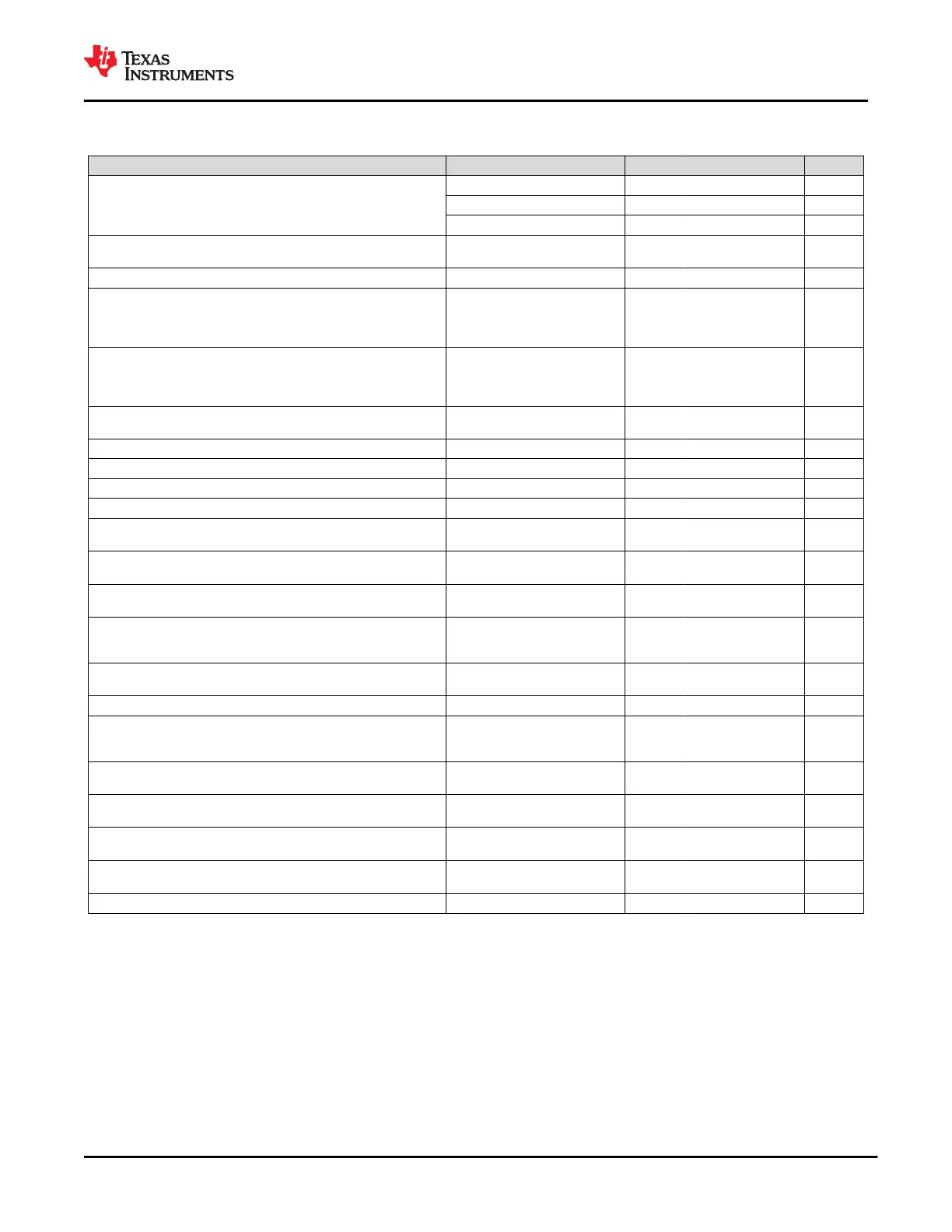
7.11 Port Power Switch Characteristics (continued)
Recommended operating conditions; T
A
= –10 to 85°C unless otherwise noted
PARAMETER TEST CONDITIONS
(3)
MIN TYP MAX UNIT
IPPCBL_ACC PP_CABLE current sense accuracy
I = 100 mA 1 A/V
I = 200 mA 1 A/V
I = 500 mA 1 A/V
IGATEEXT
(2)
External Gate Drive Current on HV_GATE1 and
HV_GATE2
4 5 6
μA
VGSEXT VGS voltage driving external FETs 4.5 7.5 V
TON_HV
PP_HV path turn on time from enable to VBUS
= 95% of PP_HV voltage
Configured as a source or as a sink
with soft start disabled. PP_HV =
20 V, CVBUS = 10 μF, ILOAD =
100 mA
8
ms
TON_5V
PP_5V0 path turn on time from enable to VBUS
= 95% of PP_5V0 voltage
Configured as a source or as a sink
with soft start disabled. PP_5V0 =
5 V, CVBUS = 10 μF, ILOAD = 100
mA
2.5
ms
TON_CC
PP_CABLE path turn on time from enable to
C_CCn = 95% of the PP_CABLE voltage
PP_CABLE = 5 V, C_CCn = 500
nF, ILOAD = 100 mA
2
ms
ISS Soft start charging current 5.5 7 8.5 μA
RSS_DIS Soft start discharge resistance 0.6 1 1.4 kΩ
VTHSS Soft start complete threshold 1.35 1.5 1.65 V
TSSDONE Soft start complete time CSS = 220 nF 31.9 46.2 60.5 ms
VREVPHV
Reverse current blocking voltage threshold for
PP_HV switch
2 6 10
mV
VREVPEXT
Reverse Current Blocking voltage Threshold for
PP_EXT external switches
2 6 10
mV
VREV5V0
Reverse current blocking voltage threshold for
PP_5V0 switches
2 6 10
mV
VHVDISPD
Voltage threshold above VIN at which the
pulldown RHVDISPD on VBUS will disable
during a transition from PHV to 5V0
45 200 250
mV
VSAFE0V
Voltage that is a safe 0 V per USB-PD
Specifications
0 0.8
V
TSAFE0V Voltage transition time to VSAFE0V 650 ms
VSO_HV
Voltage on PP_HV or PP_HVEXT above which
the PP_HV or PP_EXT to PP_5V0 transition on
VBUS will meet transition requirements
9.9
V
SRPOS
Maximum slew rate for positive voltage
transitions
0.03
V/μs
SRNEG
Maximum slew rate for negative voltage
transitions
–0.03
V/μs
TSTABLE
EN to stable time for both positive and negative
voltage transitions
275
ms
VSRCVALID
Supply output tolerance beyond VSRCNEW
during time TSTABLE
–0.5 0.5
V
VSRCNEW Supply output tolerance –5 5 %
(1) The current sense in the ADC will not accurately read below the current VREV5V0/RPP5V or VREVHV/RPPHV because of the reverse
blocking behavior. When reverse blocking is disabled, the values given for accuracy are valid.
(2) Limit the resistance from the HV_GATE1/2 pins to the external FET gate pins to < 1Ω to provide adequate response time to short
circuit events.
(3) Maximum capacitance on VBUS when configured as a source must not exceed 12 µF.
(4) Specified for a 10-mΩ RSENSE resistor and 10-mΩ RSENSE application code setting. Values will scale with a different RSENSE
resistance and application code setting.
(5) Settings selected automatically by application code for the current limit needed in the application.
www.ti.com
TPS65982
SLVSD02E – MARCH 2015 – REVISED AUGUST 2021
Copyright © 2021 Texas Instruments Incorporated
Submit Document Feedback
19
Product Folder Links: TPS65982