9.3.8 System Glue Logic
The system glue logic module performs various system interface functions such as control of the system
interface for RESETZ, MRESET, and VOUT_3V3. This module supports various hardware timers for digital
control of analog circuits.
9.3.9 Power Reset Congrol Module (PRCM)
The PRCM implements all clock management, reset control, and sleep mode control.
9.3.10 Interrupt Monitor
The Interrupt Control module handles all interrupt from the external GPIO as well as interrupts from internal
analog circuits.
9.3.11 ADC Sense
The ADC Sense module is a digital interface to the SAR ADC. The ADC converts various voltages and currents
from the analog circuits. The ADC converts up to 11 channels from analog levels to digital signals. The ADC can
be programmed to convert a single sampled value.
9.3.12 UART
Two digital UARTS are provided for serial communication. The inputs to the UART are selectable by a
programmable digital crossbar multiplexer. The UART may act as pass-through between the system and the
Type-C port or may filter through the digital core. The UART_RX/TX pins are typically used to daisy chain
multiple TPS65982s in series to share application code at startup.
9.3.13 I
2
C Slave
Two I
2
C interfaces provide interface to the digital core from the system. These interfaces are master/slave
configurable and support low-speed and full-speed signaling. See the Section 9.5.2 section for more information.
9.3.14 SPI Controller
The SPI controller provides a serial interface to an external flash memory. The recommended memory is the
W25Q80DV 8 Mbit Serial Flash Memory. A memory of at least 2 Mbit is required when the TPS65982 is using
the memory in an unshared manner. A memory of at least 8 Mbit is required when the TPS65982 is using the
memory in an shared manner. See the Section 9.5.1 section for more information.
9.3.15 Single-Wire Debugger Interface
The SWD interface provides a mechanism to directly master the digital core.
9.3.16 DisplayPort HPD Timers
To enable DisplayPort HPD signaling through PD messaging, two GPIO pins (GPIO4, GPIO5) are used as the
HPD input and output. When events occur on this pins during a DisplayPort connection through the Type-C
connector (configured in firmware), hardware timers trigger and interrupt the digital core to indicated needed
PD messaging. Table 9-5 shows each I/O function when GPIO4/5 are configured in HPD mode. When HPD
is not enabled via firmware, both GPIO4 and GPIO5 remain generic GPIO and may be programmed for other
functions. Figure 9-42 and Figure 9-43.
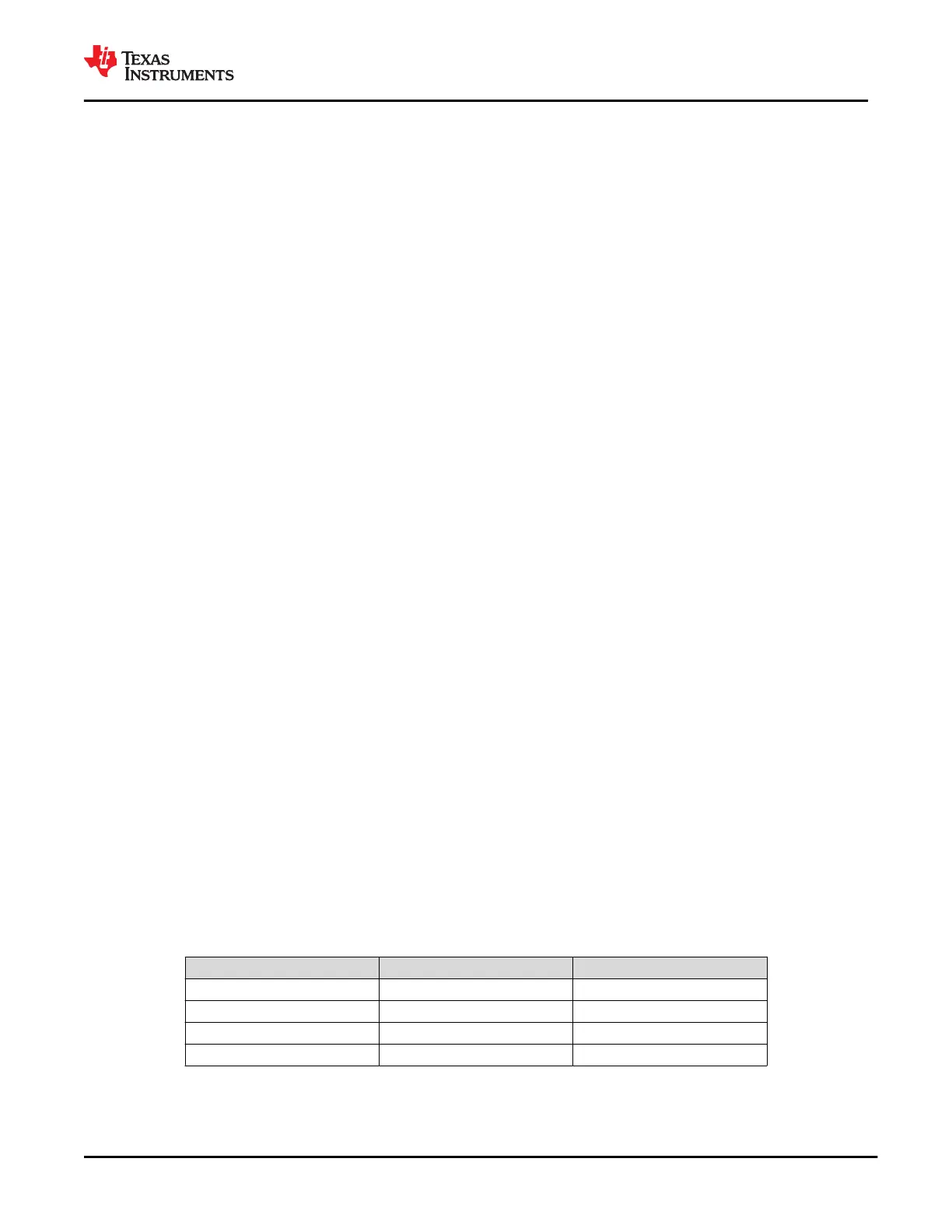
Table 9-5. HPD GPIO Configuration
HPD (Binary) Configuration GPIO4 GPIO5
00 HPD TX Generic GPIO
01 HPD RX Generic GPIO
10 HPD TX HPD RX
11 HPD TX/RX (bidirectional) Generic GPIO
www.ti.com
TPS65982
SLVSD02E – MARCH 2015 – REVISED AUGUST 2021
Copyright © 2021 Texas Instruments Incorporated
Submit Document Feedback
61
Product Folder Links: TPS65982