is converted to detect the current (IPP_EXT) that is sourced through this path by dividing by the RSENSE
resistance.
SAR ADC
Input
Mux
10 bits
Buffers
Voltage
Dividers
Thermal
Sense
I-to-V
GPIO5
C_CC1
C_CC2
BC_ID
VBUS
PP_HV
PP_5V0
PP_CABLE
VIN_3V3
VOUT_3V3
LDO_3V3
LDO_1V8A
LDO_1V8D
SENSEP
IPP_HV
IPP_5V0
SENSEP-SENSEN (IPP_EXT)
IPP_CABLE
GPIO0-8
I2C_ADDR
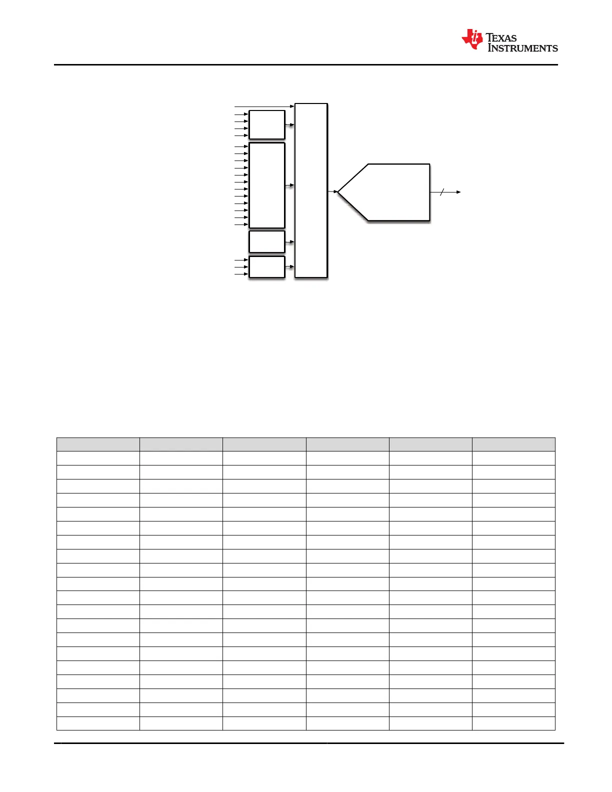
Figure 9-44. SAR ADC
9.3.17.1 ADC Divider Ratios
The ADC voltage inputs are each divided down to the full-scale input of 1.2 V. The ADC current sensing
elements are not divided.
Table 9-6 shows the divider ratios for each ADC input. The table also shows which inputs are auto-sequenced
in the round robin automatic readout mode. The C_CC1 and C_CC2 pin voltages each have two conversions
values. The divide-by-5 (CCn_BY5) conversion is intended for use when the C_CCn pin is configured as
VCONN output and the divide-by-2 (CCn_BY2) conversion is intended for use when C_CCn pin is configured as
the CC data pin.
Table 9-6. ADC Divider Ratios
CHANNEL # SIGNAL TYPE AUTO-SEQUENCED DIVIDER RATIO BUFFERED
0 Thermal Sense Temperature Yes N/A No
1 VBUS Voltage Yes 25 No
2 SENSEP Voltage Yes 25 No
3 IPP_EXT Current Yes N/A No
4 PP_HV Voltage Yes 25 No
5 IPP_HV Current Yes N/A No
6 PP_5V0 Voltage Yes 5 No
7 IPP_5V0 Current Yes N/A No
8 CC1_BY5 Voltage Yes 5 Yes
9 IPP_CABLE Current Yes N/A No
10 CC2_BY5 Voltage Yes 5 Yes
11 GPIO5 Voltage No 1 No
12 CC1_BY2 Voltage No 2 Yes
13 CC2_BY2 Voltage No 2 Yes
14 PP_CABLE Voltage No 5 No
15 VIN_3V3 Voltage No 3 No
16 VOUT_3V3 Voltage No 3 No
17 BC_ID Voltage No 3 Yes
18 LDO_1V8A Voltage No 2 No
19 LDO_1V8D Voltage No 2 No
TPS65982
SLVSD02E – MARCH 2015 – REVISED AUGUST 2021
www.ti.com
64 Submit Document Feedback
Copyright © 2021 Texas Instruments Incorporated
Product Folder Links: TPS65982