ZED-F9T-Integration Manual
4 Design
This section provides information to help carry out a successful schematic and PCB design.
Do not load Pin 4 (ANT_DETECT) with a capacitance more than 1 nF.
4.1 Pin assignment
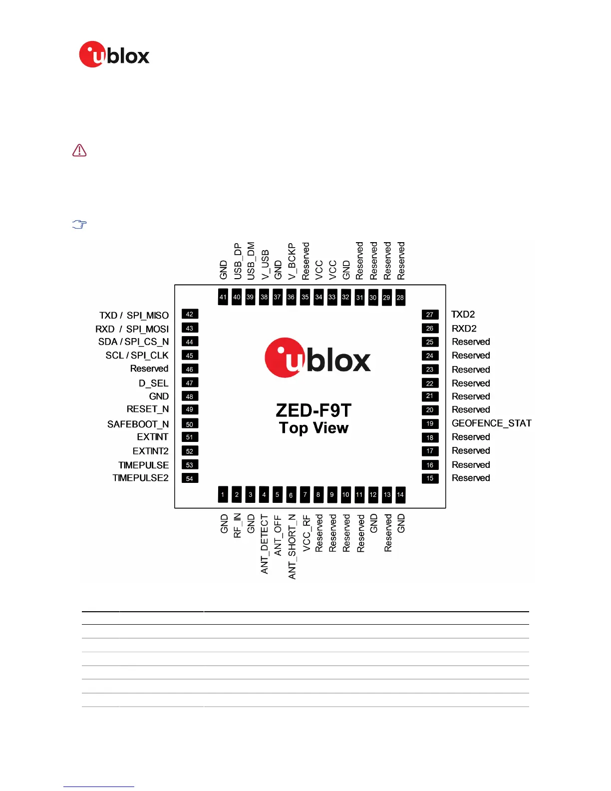
The pin assignment of the ZED-F9T module is shown in Figure 28. The defined configuration of the
PIOs is listed in Table 22.
The ZED-F9T is an LGA package with the I/O on the outside edge and central ground pads.
Figure 28: ZED-F9T pin assignment
Pin No Name I/O Description
1 GND - Ground
2 RF_IN I RF input
3 GND - Ground
4 ANT_DETECT I Active antenna detect - default active high
5 ANT_OFF O External LNA disable - default active high
6 ANT_SHORT_N I Active antenna short detect - default active low.
UBX-19005590 - R01
4 Design Page 56 of 80
Advance Information
 Loading...