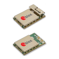
ODIN-W2 series - System integration manual
UBX-14040040 - R20 System description Page 12 of 43
C1-Public
Function Pin name Pin No. GPIO
id
Mbed pin STM32
pin
Signal description Remarks
RMII RMII_MDC C14 12 Management data
clock line
RMII_MDIO C15 13 Management data
I/O line
An external pull-up resistor is
required on the bidirectional
data signal.
RMII_TXD0 D1 20 RMII Transmit 0
RMII_TXD1 D2 21 RMII Transmit 1
RMII_TX-EN D3 22 RMII Transmit
enable
Active high.
RMII_CRS-DV D4 23
Carrier
Sense/Receive Data
Valid input
Carrier Sense and Receive Data
Valid signals are multiplexed
together; the multiplexing
scheme varies with
implementation.
RMII_RXD0 D5 24 RMII Receive 0
RMII_RXD1 D6 25 RMII Receive 1
RMII_REF-
CLK
D8 26 RMII Reference
clock input
Continuous 50 MHz reference
clock input.
IO UART3 RX A14 7 D0 PD_9 IO UART3 not used for u-blox
connectivity software
UART3 TX A15 8 D1 PD_8 IO UART3 not used for u-blox
connectivity software
UART3 CTS A16 9 D6 PD_11 IO UART3 not used for u-blox
connectivity software
UART3 RTS A17 10 D7 PD_12 IO UART3 not used for u-blox
connectivity software
RSVD C13 11 A0 PF_6 IO IO
RSVD C5 15 A4 PG_4 IO IO
SPI MISO /
SDIO D0
C6 16 D12 PE_13 IO SPI not used for
SPI SCK/
SDIO CLK
C8 17 D13 PE_12 IO SPI not used for u-blox
connectivity software
SPI MOSI /
SDIO CMD
C10 18 D11 PE_14 IO SPI not used for u-blox
connectivity software
SPI SEL C11 19 D10 PE_11 IO SPI not used for u-blox
connectivity software
IO SDIO CD C12 29 D9 PE_9 IO
RSVD
RSVD/
I2C_SCL
C17 D15 PF_1 I
2
C not used for u-blox
connectivity software
RSVD/
I2C_SDA
C18 D14 PF_0 I
2
C not used for u-blox
connectivity software
RSVD RSVD B1, B2, B3,
B4, B5, B6,
B7, B8, C2,
C9
Reserved pin. All RSVD should be left
unconnected.
Test
point
JTAG_NTRST TP5 JTAG_NTRST
PB_4 JTAG not used for u-blox
connectivity software
JTAG_TMS TP7 JTAG_TMS PA_13 JTAG not used for u-blox
connectivity software
JTAG_TDI TP8 JTAG_TDI PA_15 JTAG not used for u-blox
connectivity software
 Loading...


