ODIN-W2 series - System integration manual
UBX-14040040 - R20 Design-in Page 27 of 43
C1-Public
• Power planes should keep a distance from the PCB edge sufficient to route a ground ring around
the PCB, the ground ring must then be connected to other layers through vias.
⚠ The heat dissipation during continuous transmission at maximum power can significantly raise
the temperature of the application base-board below the ODIN-W2 series modules. Avoid placing
temperature sensitive devices close to the ODIN-W2 series module and provide adequate
grounding of the module to transfer to the PCB the generated heat.
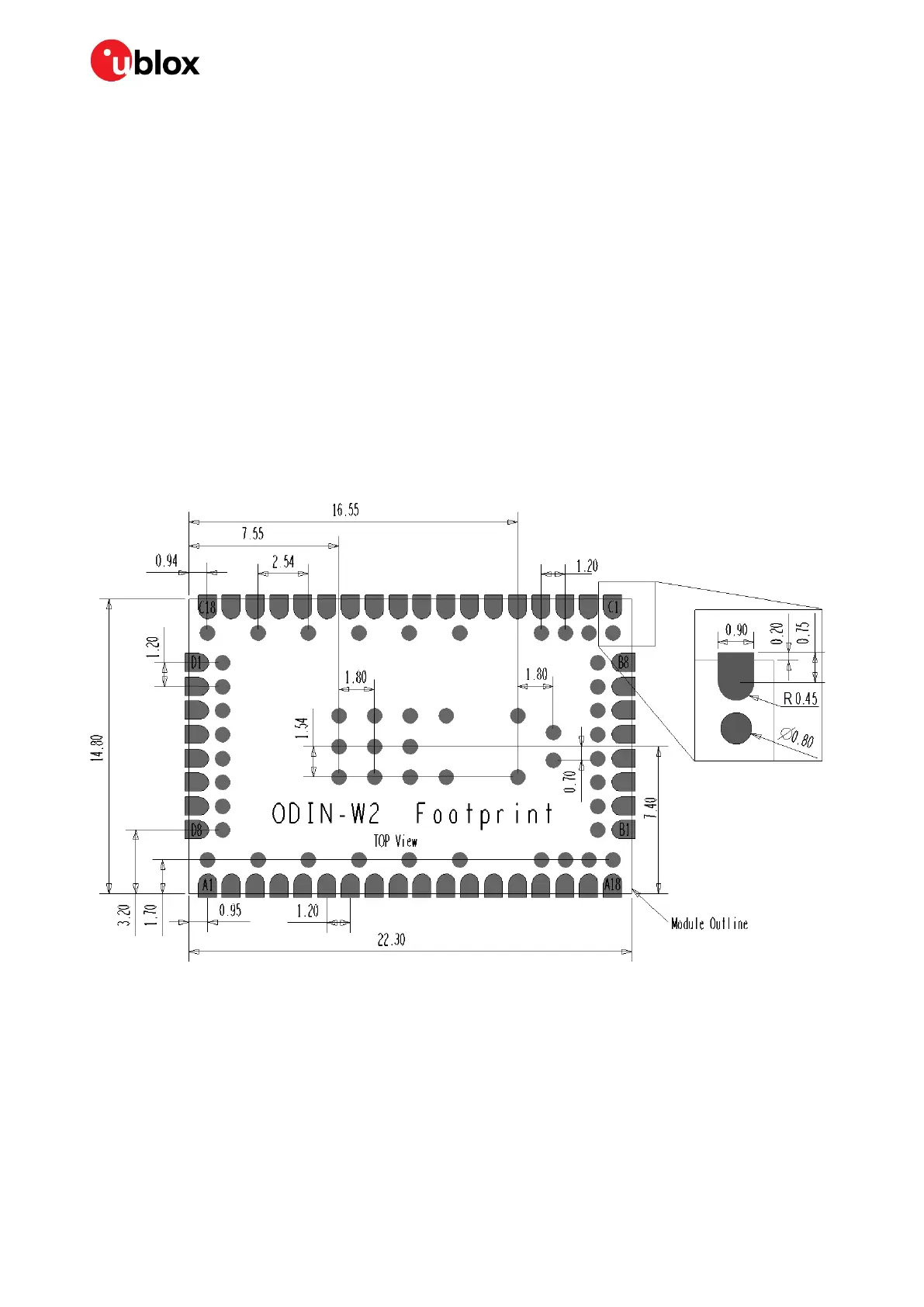
3.7 Module footprint and paste mask
Figure 9 describes the suggested footprint (that is, copper mask) layout for the ODIN-W2 series
modules. The proposed land pattern layout reflects the pads layout of the modules and extends 0.2
mm outside the module outline.
The Non Solder Mask Defined (NSMD) pad type is recommended over the Solder Mask Defined (SMD)
pad type, which implements the solder mask opening 50 μm larger per side than the corresponding
copper pad.
The suggested paste mask layout for the ODIN-W2 series modules is to follow the copper mask layout
as described in Figure 9.
Figure 9: ODIN-W2 series footprint
☞ These are recommendations only and not specifications. The exact mask geometries, distances
and stencil thicknesses must be adapted to the specific production processes (for example,
soldering and so on) of the customer.
3.8 Thermal guidelines
The ODIN-W2 series modules have been successfully tested in -40 °C to +85 °C. The board will
generate heat during high loads that must be dissipated to sustain the life time of the components.
 Loading...


