SARA-G450 - System integration manual
UBX-18046432 - R08 Design-in Page 61 of 143
C1-Public
2.2.1.3 Guidelines for VCC supply circuit design using a LDO linear regulator
The use of a linear regulator is suggested when the difference from the available supply rail and the
VCC value is low: linear regulators provide high efficiency when transforming a 5 V supply to a voltage
value within the module’s VCC normal operating range.
The characteristics of the LDO linear regulator connected to the VCC pins should meet the following
prerequisites to comply with the module VCC requirements summarized in Table 6:
Power capabilities: the LDO linear regulator with its output circuit must be capable of providing a
stable voltage value to the VCC pins and of delivering to VCC pins the specified maximum
peak / pulse current with 1/8 duty cycle (see the SARA-G450 data sheet [1]).
Power dissipation: the power handling capability of the LDO linear regulator must be checked to
limit its junction temperature to the maximum rated operating range (i.e. check the voltage drop
from the maximum input voltage to the minimum output voltage to evaluate the power dissipation
of the regulator).
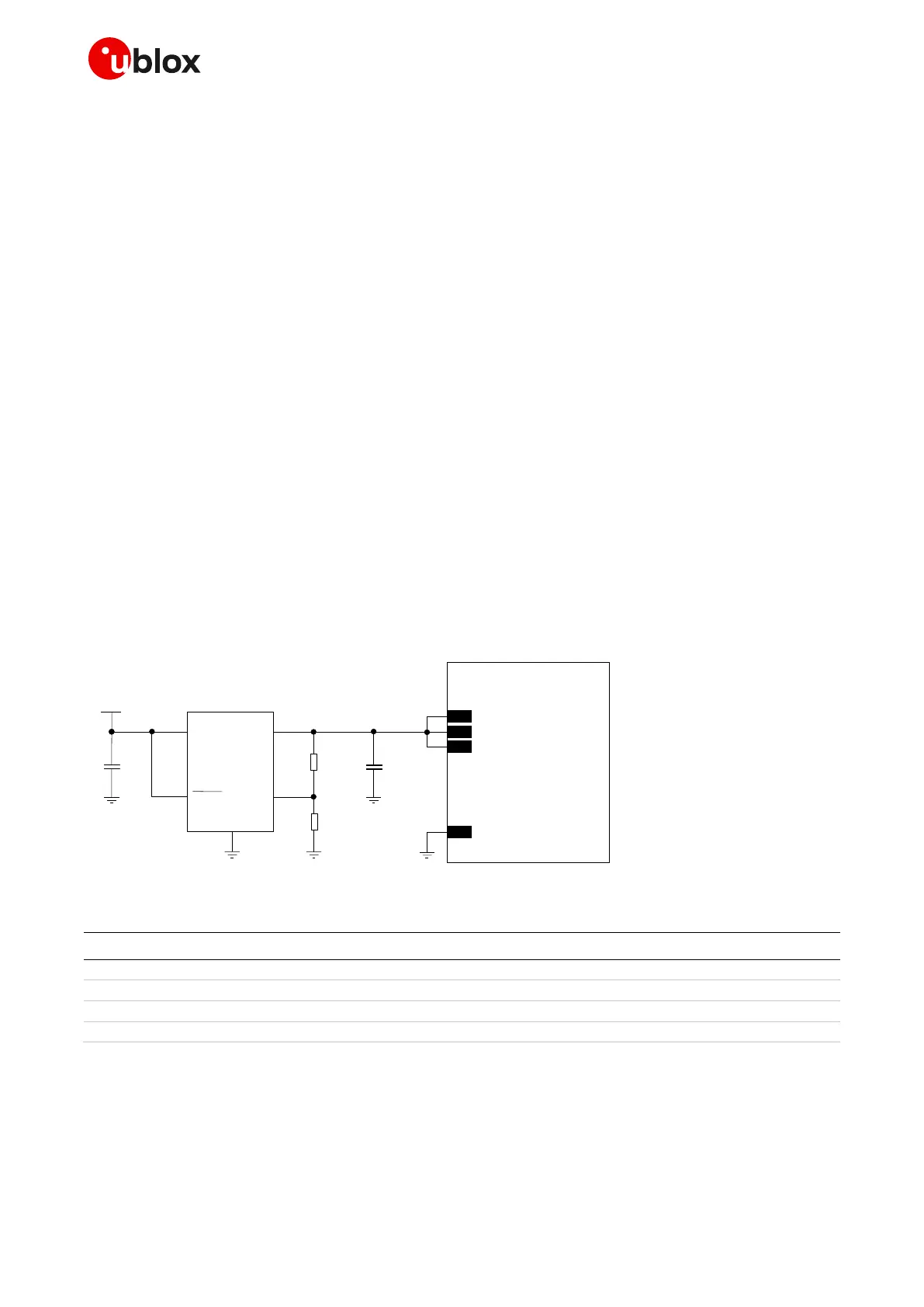
Figure 25 and the components listed in Table 15 show an example of a high reliability power supply
circuit, where the VCC module supply is provided by an LDO linear regulator capable of delivering the
specified highest peak / pulse current, with an appropriate power handling capability. The regulator
described in this example supports a wide input voltage range, and it includes internal circuitry for
reverse battery protection, current limiting, thermal limiting and reverse current protection.
It is recommended to configure the LDO linear regulator to generate a voltage supply value slightly
below the maximum limit of the module VCC normal operating range (e.g. ~4.1 V as in the circuit
described in Figure 25 and Table 15). This reduces the power on the linear regulator and improves the
whole thermal design of the supply circuit.
5V
C1
IN
OUT
ADJ
GND
1
2
4
5
3
C2R1
R2
U1
SHDN
SARA-G450
52
VCC
53
VCC
51
VCC
GND
Figure 25: Suggested schematic design for the VCC voltage supply application circuit using an LDO linear regulator
Part number - Manufacturer
10 µF capacitor ceramic X5R 0603 20% 6.3 V
GRM188R60J106ME47 - Murata
9.1 k resistor 0402 5% 0.1 W
RC0402JR-079K1L - Yageo Phycomp
3.9 k resistor 0402 5% 0.1 W
RC0402JR-073K9L - Yageo Phycomp
LDO linear regulator ADJ 3.0 A
LT1764AEQ#PBF - Linear Technology
Table 15: Suggested components for the VCC voltage supply application circuit using an LDO linear regulator
 Loading...