SARA-G450 - System integration manual
UBX-18046432 - R08 Design-in Page 64 of 143
C1-Public
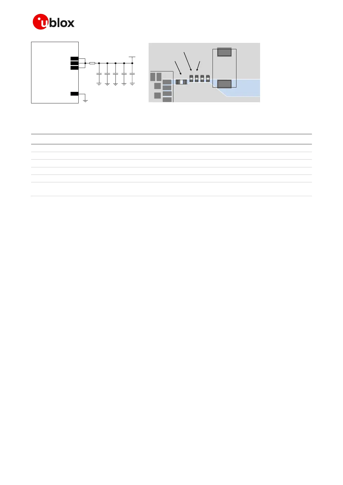
C1
GND plane
VCC line
Capacitor with
SRF ~900 MHz
C5 C3 C2
FB1
Ferrite bead
for GHz noise
C4
C5
GND
C4 C2
SARA-G450
52
VCC
53
VCC
51
VCC
3V8
C1
+
FB1
C3
Capacitor with
SRF ~1900 MHz
SARA-G450
Figure 27: Suggested schematic and layout design for the VCC line, highly recommended when using an integrated antenna
(ferrite bead is not strictly required)
Part number - Manufacturer
330 µF capacitor tantalum D_SIZE 6.3 V 45 m
T520D337M006ATE045 - KEMET
100 nF capacitor ceramic X7R 0402 10% 16 V
GRM155R71C104KA01 - Murata
10 nF capacitor ceramic X7R 0402 10% 16 V
GRM155R71C103KA01 - Murata
15 pF capacitor ceramic C0G 0402 5% 25 V
GRM1555C1E150JA01 - Murata
56 pF capacitor ceramic C0G 0402 5% 25 V
GRM1555C1E560JA01 - Murata
Chip Ferrite bead EMI filter for GHz band noise
220 at 100 MHz, 260 at 1 GHz, 2000 mA
Table 17: Suggested components to reduce ripple / noise on VCC and to avoid undershoot / overshoot on VCC voltage drops
☞ ESD sensitivity rating of the VCC supply pins is 1 kV (Human Body Model according to
JESD22-A114). A higher protection level can be required if the line is externally accessible on the
application board, e.g. if accessible battery connector is directly connected to VCC pins. A higher
protection level can be achieved by mounting an ESD protection (e.g. EPCOS CA05P4S14THSG
varistor array) close to the accessible points.
2.2.1.7 Additional guidelines for VCC separate supply circuit design
SARA-G450 modules provide separate supply inputs over the VCC pins (see Figure 3):
VCC pins #52 and #53: supply input for the internal RF power amplifier, demanding most of the
total current drawn of the module when RF transmission is enabled during a voice call or a data
transmission
VCC pin #51: supply input for the internal baseband PMU and transceiver, demanding minor
current
All the VCC pins are in general intended to be connected to the same external power supply circuit,
but separate supply sources can be implemented for specific (e.g. battery-powered) applications
considering that the voltage at the VCC pins #52 and #53 can drop to a value lower than the one at
VCC pin #51, keeping the module still switched-on and functional. Figure 28 and Table 18 describe a
possible application circuit.
 Loading...