SARA-G450 - System integration manual
UBX-18046432 - R08 Design-in Page 76 of 143
C1-Public
o It is highly recommended to strictly follow the detailed and specific guidelines provided by the
antenna manufacturer regarding correct installation and deployment of the antenna system,
including PCB layout and matching circuitry.
o Further to the custom PCB and product restrictions, the antenna may require tuning to obtain
the required performance for compliance with the applicable certification schemes. It is
recommended to ask the antenna manufacturer for the design-in guidelines related to the
custom application.
In both cases, selecting an external or an internal antenna, observe these recommendations:
Select an antenna providing optimal return loss (or VSWR) figure over all the operating
frequencies.
Select an antenna providing optimal efficiency figure over all the operating frequencies.
Select an antenna providing appropriate gain figure (i.e. combined antenna directivity and
efficiency figure) so that the electromagnetic field radiation intensity do not exceed the regulatory
limits specified in some countries.
2.4.1.2 Guidelines for antenna RF interface design
Guidelines for ANT pin RF connection design
Correct transition between the ANT pin and the application board PCB must be provided,
implementing the following design-in guidelines for the layout of the application PCB close to the pad
designed for the ANT pin:
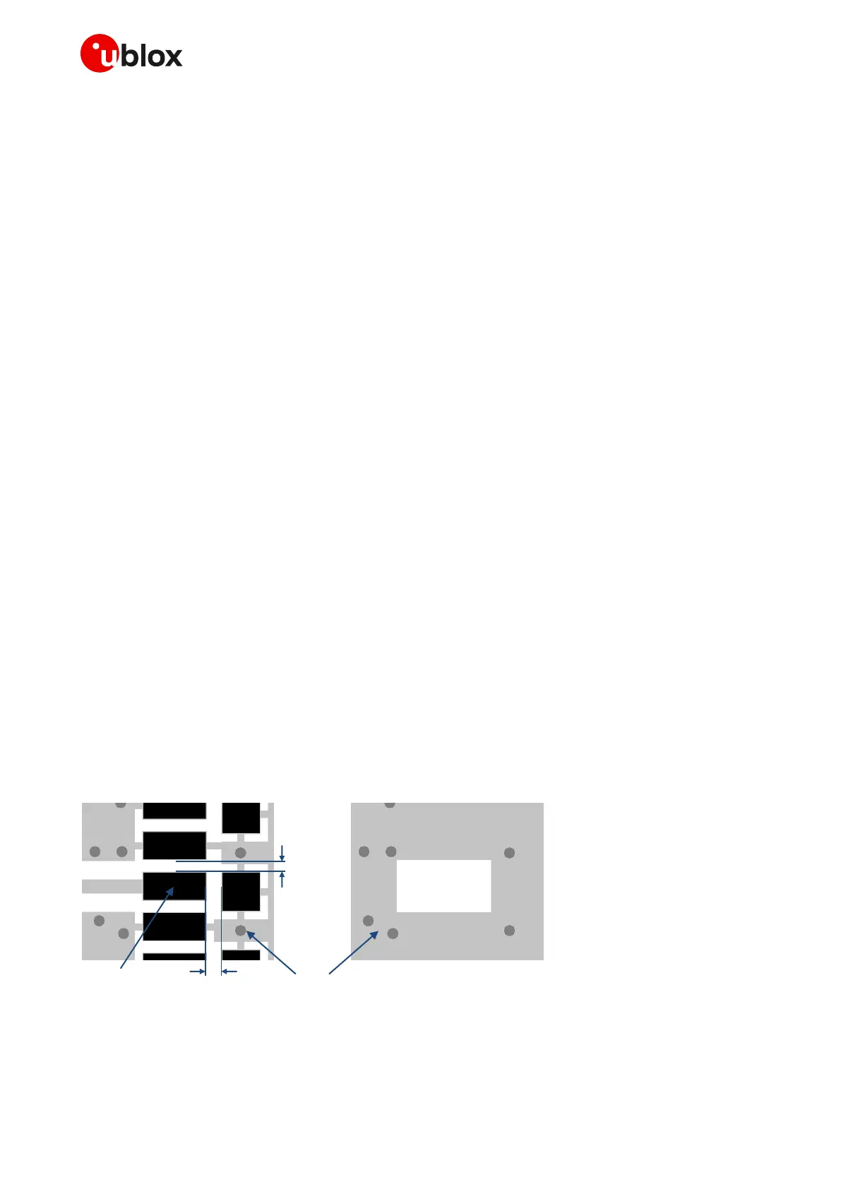
On a multi-layer board, the whole layer stack below the RF connection should be free of digital lines
Increase ground keep-out (i.e. clearance, a void area) around the ANT pad, on the top layer of the
application PCB, to at least 250 µm up to adjacent pads metal definition and up to 400 µm on the
area below the module, to reduce parasitic capacitance to ground, as described in the left picture
in Figure 37
Add ground keep-out (i.e. clearance, a void area) on the buried metal layer below the ANT pad if the
top-layer to buried layer dielectric thickness is below 200 µm, to reduce parasitic capacitance to
ground, as described in the right picture in Figure 37
Min.
250 µm
Min. 400 µm
GND
ANT
GND clearance
on very close buried layer
below ANT pad
GND clearance
on top layer
around ANT pad
Figure 37: GND keep-out area on the top layer around ANT pad and on the very close buried layer below ANT pad
 Loading...