SARA-G450 - System integration manual
UBX-18046432 - R08 Design-in Page 79 of 143
C1-Public
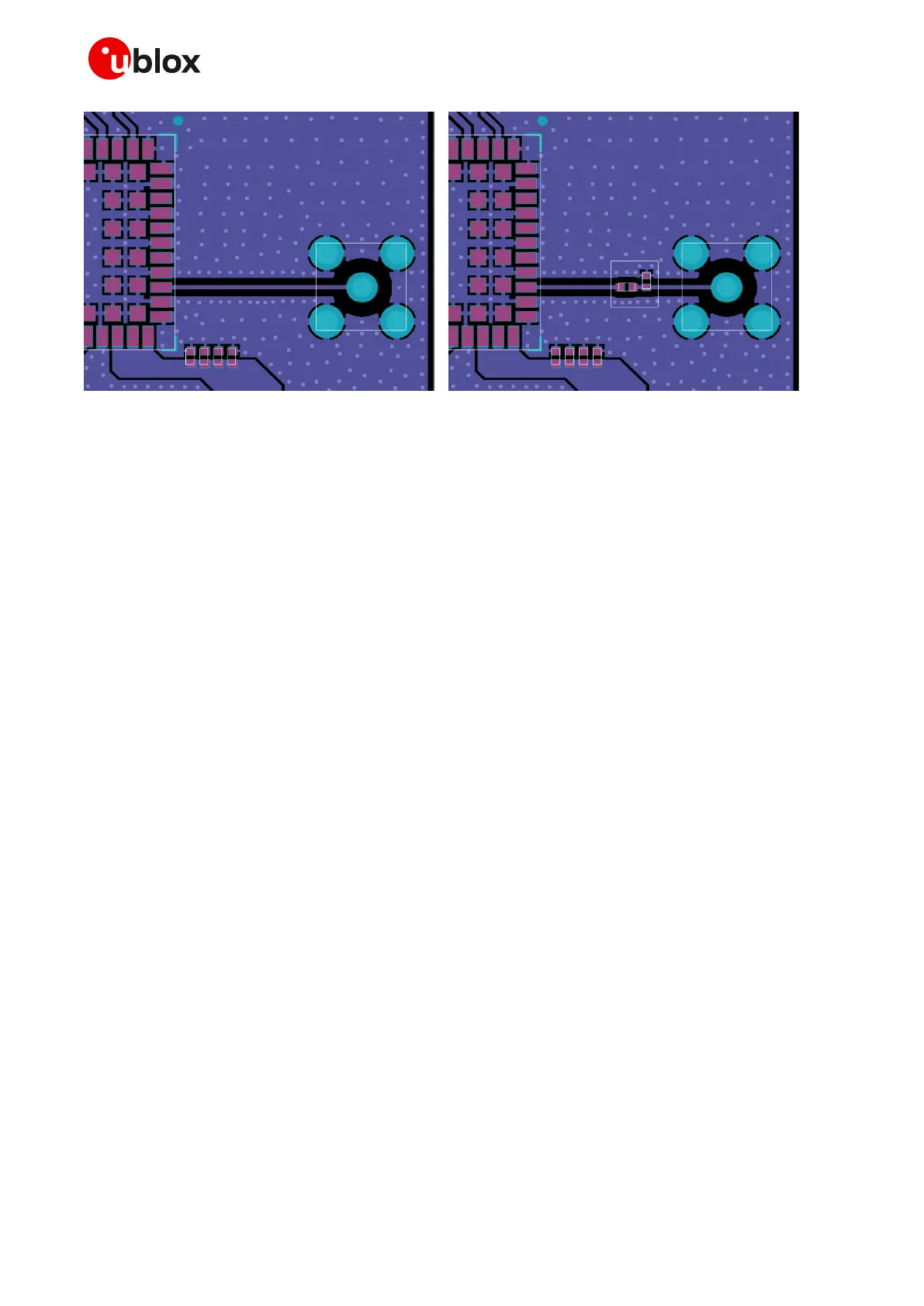
SARA module
SMA
connector
SARA module
SMA
connector
High-pass filter for
ANT port
ESD immunity increase
Figure 40: Suggested circuit and layout for antenna RF circuit on application board, if antenna detection is not required
Guidelines for RF termination design
The RF termination must provide a characteristic impedance of 50 as well as the RF transmission
line up to the RF termination itself, to match the characteristic impedance of the module ANT pin.
However, real antennas do not have a perfect 50 load on all the supported frequency bands.
Therefore, to reduce performance degradation due to antenna mismatch as much as possible, the RF
termination must provide optimal return loss (or VSWR) figure over all the operating frequencies, as
summarized in Table 7.
If an external antenna is used, the antenna connector represents the RF termination on the PCB:
Use a suitable 50 connector providing a clean PCB-to-RF-cable transition.
Strictly follow the connector manufacturer’s recommended layout, for example:
o SMA Pin-Through-Hole connectors require ground keep-out (clearance, a void area) on all the
layers around the central pin up to annular pads of the four GND posts, as shown in Figure 40.
o U.FL surface mounted connectors require no conductive traces (i.e. clearance, a void area) in
the area below the connector between the GND land pads.
Cut out the ground layer under RF connectors and close to buried vias, to remove stray
capacitance and thus keep the RF line at 50 : e.g. the active pad of U.FL connectors needs to
have a ground keep-out (i.e. clearance, a void area) at least on first inner layer to reduce parasitic
capacitance to ground.
If an integrated antenna is used, the RF termination is represented by the integrated antenna itself:
Use an antenna designed by an antenna manufacturer, providing the best possible return loss (or
VSWR).
Provide a ground plane large enough according to the related integrated antenna requirements:
the ground plane of the application PCB can be reduced to a minimum size that must be similar to
one quarter of wavelength of the minimum frequency to be radiated. As numerical example:
Frequency = 824 MHz Wavelength = 36.4 cm Minimum ground plane size = 9.1 cm
It is highly recommended to strictly follow the detailed and specific guidelines provided by the
antenna manufacturer regarding correct installation and deployment of the antenna system,
including PCB layout and matching circuitry.
Further to the custom PCB and product restrictions, the antenna may require a tuning to comply
with all the applicable required certification schemes. It is recommended to consult the antenna
manufacturer for the design-in guidelines for the antenna related to the custom application.
 Loading...