SARA-R5 series - System integration manual
UBX-19041356 - R04 Design-in Page 63 of 118
C1-Public
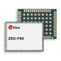
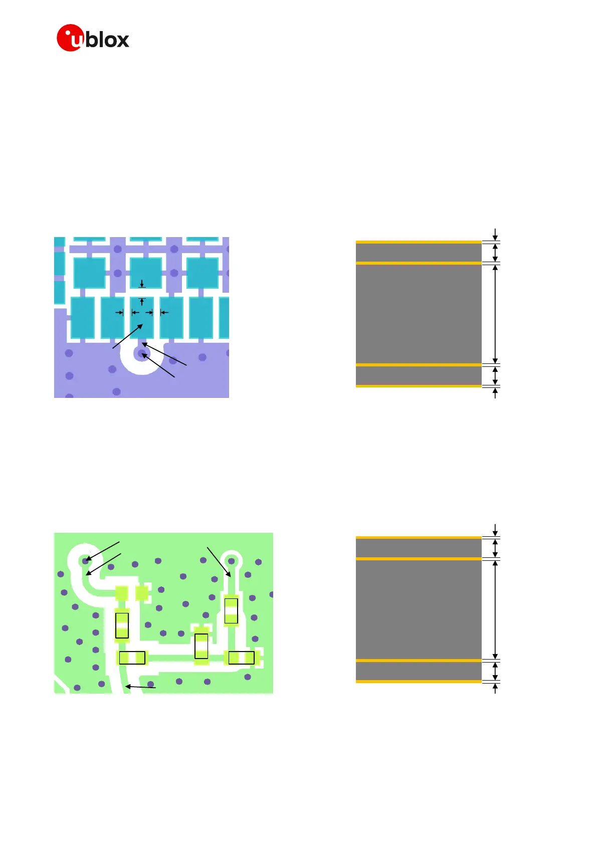
The u-blox host printed circuit board has a structure of 4 copper layers with 35 m thickness (1 oz/ft
2
)
each, using FR4 dielectric substrate material with 4.3 typical permittivity at 1 GHz, and 0.013 typical
loss tangent at 1 GHz.
The top layer layout of the u-blox host PCB designed to accommodate the ANT pad of SARA-R5 series
module is described in Figure 38: the left side illustrates top layer copper mask and top layer solder
resist mask, with top layer to bottom layer vias; the right side illustrates the PCB stack-up structure.
Considering that the thickness of the dielectric material from the top layer to the buried layer is larger
than 200 m, no GND keep-out is implemented on the buried metal layer area below the ANT pad.
Guidelines to design an equivalent proper connection for the ANT pad on a host printed circuit board
are available in section 2.4.1.1.
Figure 38: Top layer layout and stack-up structure of the u-blox host PCB for the ANT pad of the module
As illustrated on the left side of Figure 38, the antenna RF trace is routed from the RF pad on the top
layer (L1) to the bottom layer (L4) through a dedicated via. After the via, the antenna RF trace, as 50
transmission line, is connected to the antenna detection circuit described in Figure 37 and Table 21,
with the layout illustrated on the left side of Figure 39. Guidelines to design a proper equivalent
(optional) antenna detection circuit on a host printed circuit board are available in section 2.4.5.

 Loading...