Platform Cable USB II
DS593 (v1.2.1) March 17, 2011 www.xilinx.com
21
Input Receive Structure
Each input signal is routed through a NC7WZ07 ultra high-speed CMOS, open-drain receive buffer. Series-termination
resistors (499Ω) provide current limit protection for positive and negative excursions. Schottky diodes provide the input
buffers with undershoot protection. The receive buffers are biased by an internal 1.8V power supply. See Table 9, page 32
for V
IL
and V
IH
specifications. The receive buffers can tolerate voltages higher than the bias voltage without damage,
compensating for target system drivers in multi-device chains where the last device in the chain might be referenced to a
voltage other than V
REF
(for example, the TDO output at the end of a JTAG chain).
X-Ref Target - Figure 21
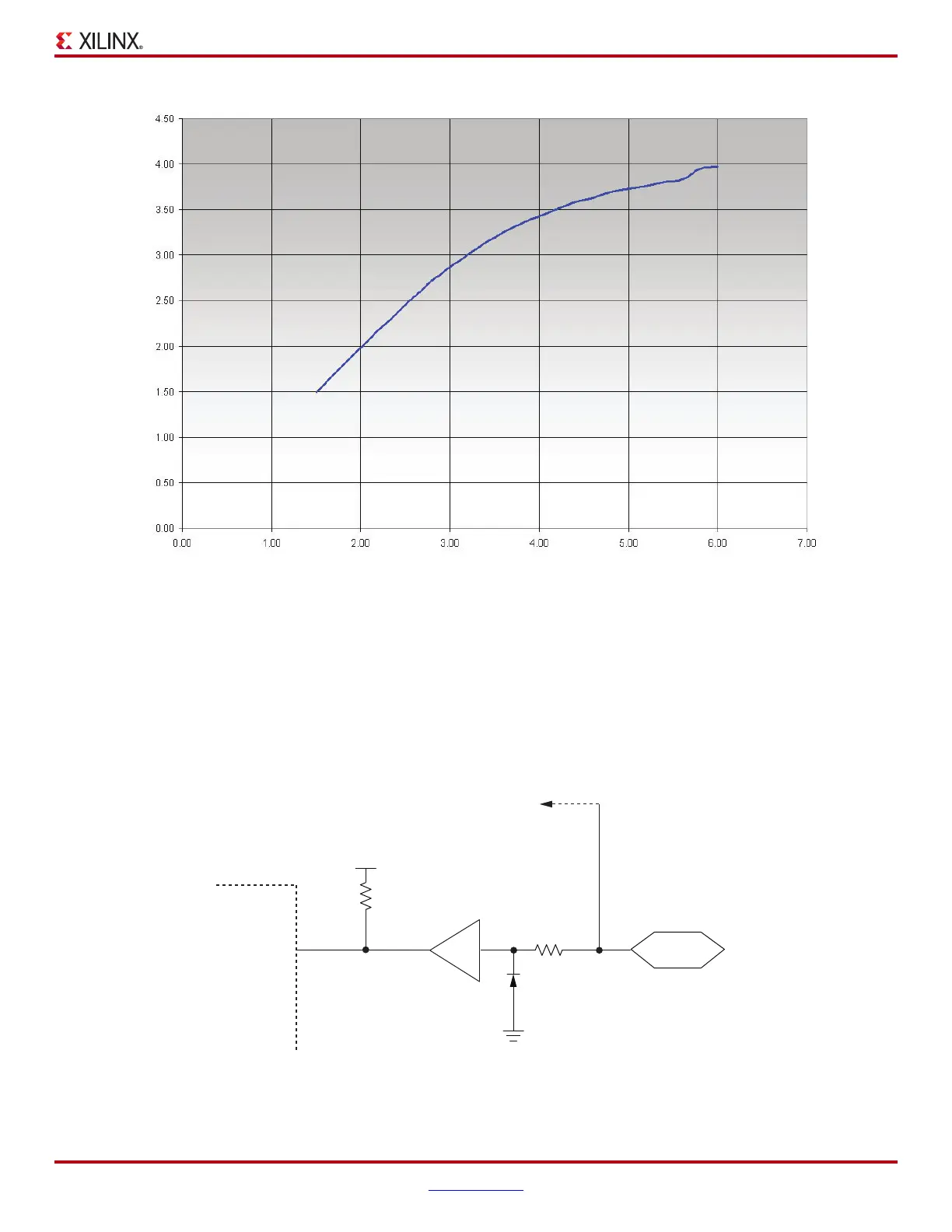
Figure 21: Output Drive Voltage vs. V
REF
X-Ref Target - Figure 22
Figure 22: Target Interface Receiver Topology
Output Drive Voltage (V)
V
REF
Voltage (VDC)
DS593_21_021408
FPGA
NC7WZ07
Input
I/O Pin
2 mm Connector
BAT54
499Ω
To output buffer
DS593_22_021408