Platform Cable USB II
DS593 (v1.2.1) March 17, 2011 www.xilinx.com
31
Platform Cable USB II Operating Characteristics
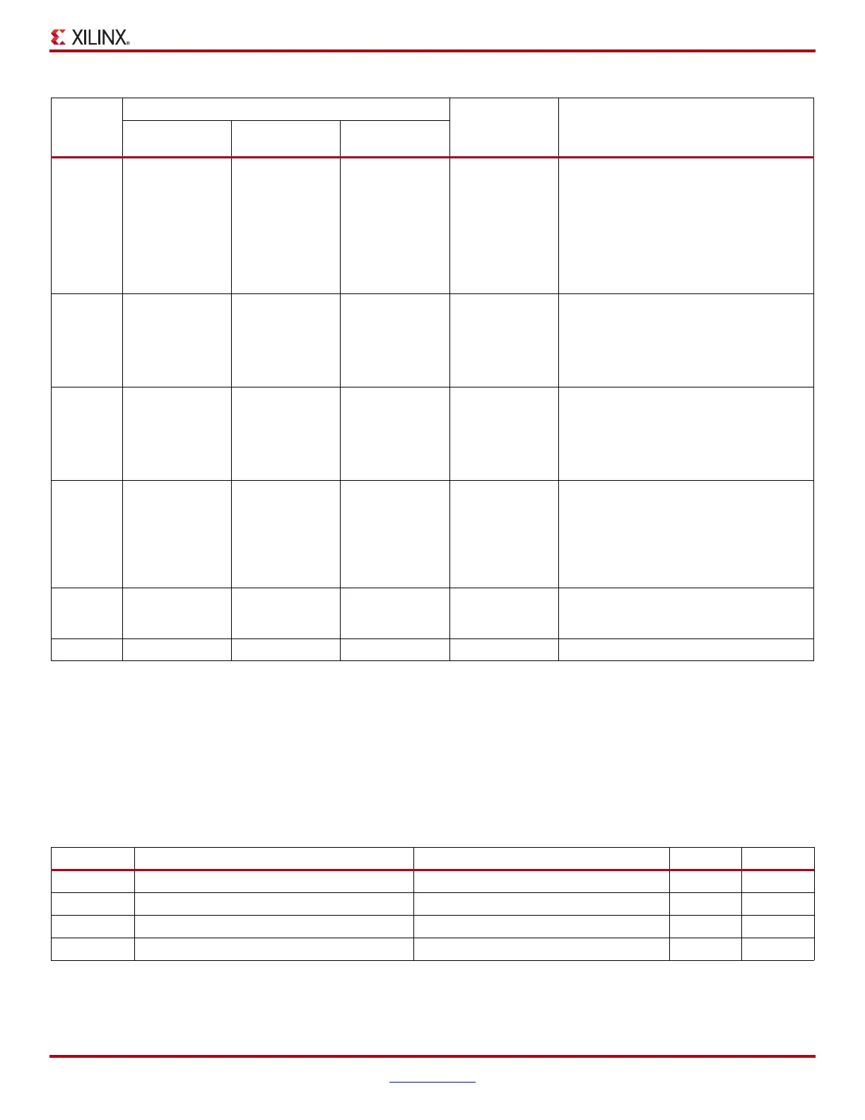
8– – Done In
Slave Serial Configuration Done. This pin
indicates to Platform Cable USB II that
target FPGAs have received the entire
configuration bitstream and should be
connected to the Done pin on all FPGAs in
parallel for daisy-chained configurations.
Additional CCLK cycles are issued following
the positive transition of Done to insure that
the configuration process is complete.
10 – – DIN Out
Slave Serial Configuration Data Input.
This pin outputs the serial input data stream
for target FPGAs and should be connected
to the DIN pin of the target FPGA in a single-
device system, or to the DIN pin of the first
FPGA in a daisy-chain configuration.
13 – – PGND Out
Slave Serial Pseudo Ground. Use of this
pin is optional. PGND is pulled Low during
Slave Serial operations; otherwise, it is high-
Z. This pin is connected to an open-drain
driver and requires a pull-up resistor on the
target system.
(4)
14 – – INIT In
Slave Serial Configuration Initialization.
This pin indicates that configuration memory
is being cleared and should be connected to
the INIT_B pin of the target FPGA for a
single-device system, or to the INIT_B pin
on all FPGAs in parallel in a daisy-chain
configuration.
3, 5, 7, 9,
11
––––
Digital Ground. All ground pins should be
connected to digital ground on the target
system to minimize crosstalk.
1, 12 – – – – Not Connected.
Notes:
1. The listed SPI pin names match those of SPI flash devices from ST Microelectronics. Pin names of compatible SPI devices from other
vendors can vary. Consult the vendor's SPI device data sheet for equivalent pin names.
2. The signal pins (HALT_INIT_WP, TDI_DIN_MOSI, TDO_DONE_MISO, TCK_CCLK_SCK, TMS_PROG_SS) are bidirectional. Their
directions during cable operations are defined by the current configuration or programming mode (JTAG, SPI or Slave Serial).
3. The target reference voltage must be regulated and not have a current-limiting resistor in series with the V
REF
pin.
4. For more details, see Target System Connections, page 15 and Pseudo Ground Signal, page 22.
Tabl e 7 : Absolute Maximum Ratings
(1)
Symbol Description Conditions Value Units
V
BUS
USB Port Supply Voltage 5.25 V
V
REF
Target Reference Voltage 6.00 V
I
REF
Target Supply Current V
REF
= 5.25V 100 mA
T
A
Ambient Operating Temperature 70 ° C
Tabl e 6 : JTAG/SPI/Slave Serial Port: 2-mm Connector Signals (Cont’d)
Pin
Number
MODE
Direction
(2)
Description
JTAG
Configuration
SPI
Programming
(1)
Slave-Serial
Configuration