SP605 Hardware User Guide www.xilinx.com 11
UG526 (v1.1.1) February 1, 2010
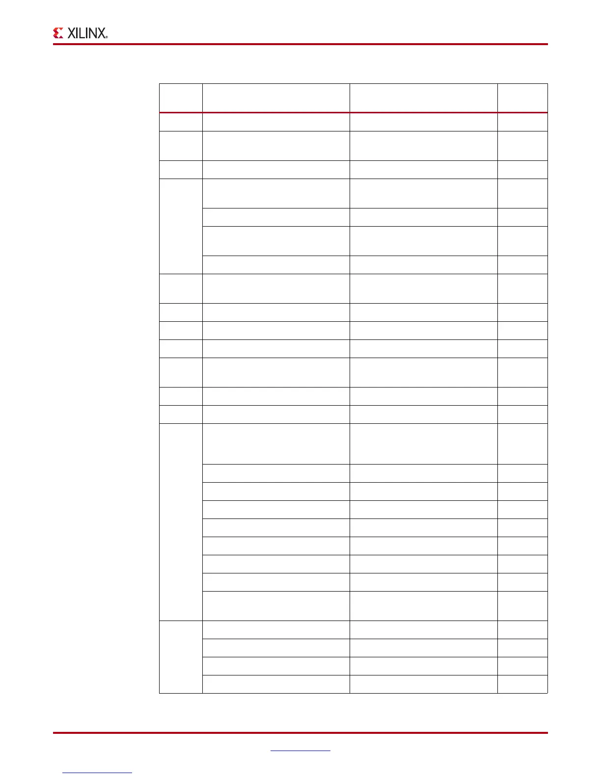
Detailed Description
4 Linear BPI Flash x16 Numonyx JS28F256P30T95 19
5
SystemACE CompactFlash
Socket
XCCACE-TQ144I Controller 20
6 USB JTAG Conn. (USB Mini-B) USB JTAG Download Circuit 32
7
Clock Generation
200 MHz OSC, oscillator socket,
SMA connectors
13, 14
a. 200 MHz oscillator Epson 200 MHz 2.5V LVDS 14
b. Oscillator socket, single-
ended, LVCMOS
MMD Components 2.5V 27 MHz 14
c. SMA connectors SMA pair P(J41) / N(J38) 13
8
GTP port SMA x4 and
MGT Clocking SMA (REFCLK)
MGT RX,TX Pairs x4 SMA MGT
REFCLK x2 SMA
13
9 PCIe 1-lane edge conn.(Gen 1) Card Edge Connector, 1-lane 12
10 SFP Module Cage/Connector AMP 136073-1 12
11 Ethernet 10/100/1000 Marvell M88E1111 EPHY 11
12
USB UART (USB-to-UART
Bridge)
Silicon Labs CP2103GM 15
13 DVI Codec and Video Connector Chrontel CH7301C-TF 16,17
14 IIC EEPROM (on backside) ST Micro M24C08-WDW6TP 15
15
Status LEDs
10, 11, 14,
18, 20, 25,
27, 31, 33
a. FMC Power Good 10
b. System ACE CF Status 11
c. FPGA INIT and DONE 14
d. Ethernet PHY Status 18
e. JTAG USB Status 20
f. FPGA Awake 27
g. TI Power Good 31
h. MGT AVCC, DDR3 Term
Pwr Good
33
16
a. User LEDs (4) Red LEDs (active-High) 14
b. User Pushbuttons (4) Active-High 14
c. User DIP Switch (4-pole) 4-pole (active-High) 14
d. User SMA (2) GPIO x2 SMA 13
Table 1-1: SP605 Features (Cont’d)
Number Feature Notes
Schematic
Page
 Loading...


