16 www.xilinx.com SP605 Hardware User Guide
UG526 (v1.1.1) February 1, 2010
Chapter 1: SP605 Evaluation Board
3. SPI x4 Flash
The Xilinx Spartan-6 FPGA hosts a SPI interface which is visible to the Xilinx iMPACT
configuration tool. The SPI memory device operates at 3.0V; the Spartan-6 FPGA I/Os are
3.3V tolerant and provide electrically compatible logic levels to directly access the SPI flash
through a 2.5V bank. The XC6SLX45T-3FGG484 is a master device when accessing an
external SPI flash memory device.
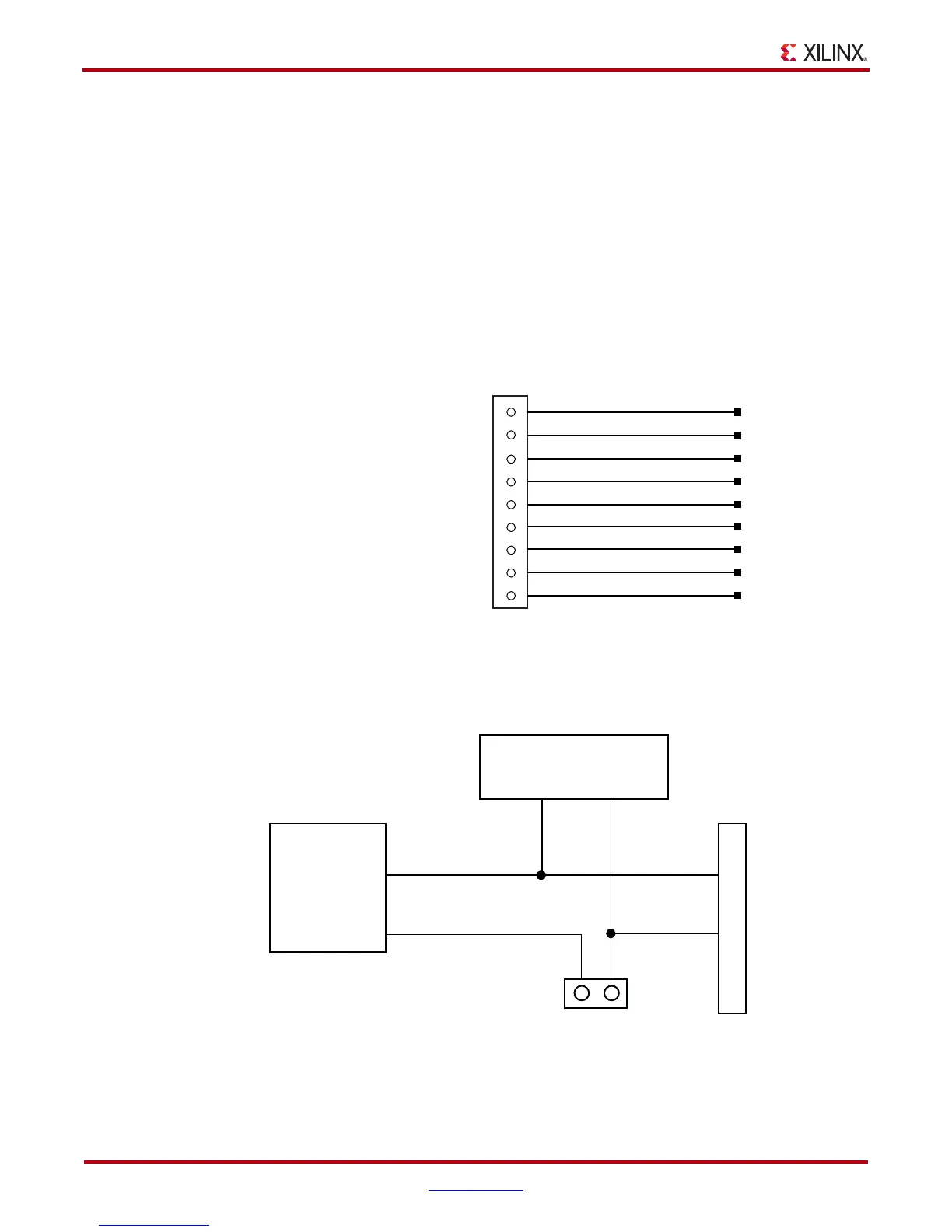
The SP605 SPI interface has two parallel connected configuration options (Figure 1-3): an
SPI X4 (Winbond W25Q64VSFIG) 64-Mb flash memory device (U32) and a flash
programming header (J17). J17 supports a user-defined SPI mezzanine board. The SPI
configuration source is selected via SPI select jumper J46. For details on configuring the
FPGA, see “Configuration Options.”
X-Ref Target - Figure 1-3
Figure 1-3: J17 SPI Flash Programming Header
X-Ref Target - Figure 1-4
Figure 1-4: SPI Flash Interface Topology
SPI Prog
FPGA_D1_MISO2
J17
1
2
3
4
5
6
7
8
9
FPGA_D2_MISO3
FPGA_PROG_B
FPGA_MOSI_CSI_B_MISO0
SPI_CS_B
FPGA_CCLK
FPGA_D0_DIN_MISO_MISO1
UG526_03_092409
GND
VCC3V3
Silkscreen
TMS
TDI
TDO
TCK
GND
3V3
HDR_1X9
U1
FPGA SPI Interface
U32
J17
SPI x4
Flash
Memory
Winbond
W25Q64VSFIG
SPI Program
Header
SPI Select
Jumper
ON = SPI X4 U32
OFF = SPI EXT. J17
SPIX4_CS_B
DIN, DOUT, CCLK
SPI_CS_B
2
J46
1
UG526_04_092409
 Loading...


