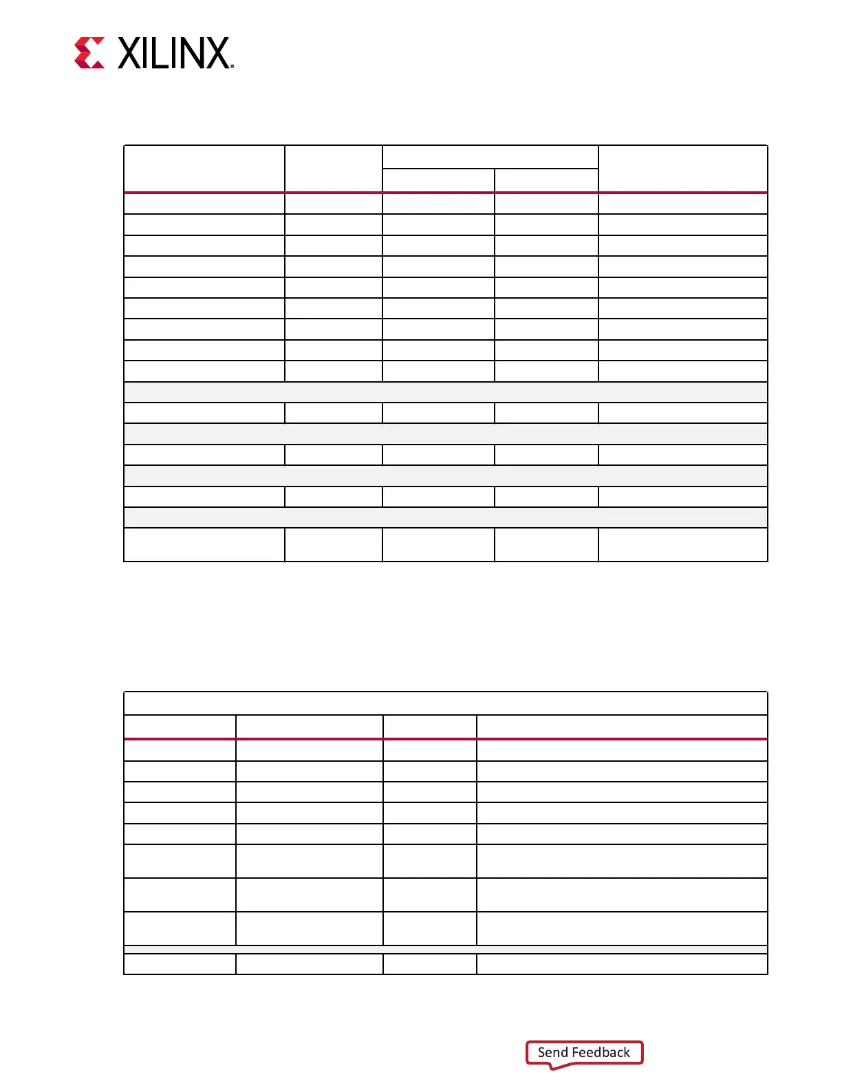
Table 9: XC7S100 U1 FPGA I2C Bus Connectivity
I2C0 Bus
I2C Switch
Position
I2C Address
Target Device
Binary Format Hex Format
TCA9548 8-Chan. Switch U23 N/A
0b1110100 0x74
U23 TCA9548A
I2C01_EEPROM_SDA/SCL 0
0b1010000 0x50
U27 M24C32
I2C02_SYSOSC_SDA/SCL 1
0b1010101 0x55
U45 SI570
I2C03_12VMON_SDA/SCL 2
0b1000001 0X41
U32 INA226
I2C04_1VMON_SDA/SCL 3
0b1000100 0x44
U33 INA226
I2C05_SYSMON_SDA/SCL 4 N/A N/A TP10/TP11 TEST POINT
I2C06_MP5470_SDA/SCL 5
0b1101000 0x68
U34 MP5470GL PMIC
I2C07_FMC_SDA/SCL 6
0b1010000 0x50
J21 FMC LPC
NOT USED 7 N/A N/A N/A
XC7S100 FPGA U1 BANK 33 I2C Port
I2C2_CAM_SDA/SCL U1.AE13/AD13
0b1101000 0x78
J8 MIPI-CSI
XC7S100 FPGA U1 BANK 13 I2C Port
I2C3_DSI_SDA/SCL U1.AB24/AC26
0bTBD 0xTBD
J20 MIPI-DSI
XC7S100 FPGA U1 BANK 15 I2C Port
I2C4_HDMI_SDA/SCL U1.K23/J24
0b1100010 0x72
U18 ADV7511 HDMI
MSP430 U25 PORT P4_1, P4_2 I2C_MSP430_SDA/SCL Bus
TCA6416 Dual 8-bit I/O Port
U24
N/A
0b0100000 0x40
U24 TCA6416A
The MSP430 system controller U25 has a local I2C_MSP430_SDA/SCL bus connected to a dual
8-bit port TI TCA6416A I/O expander U24 (address 0x40). The I/O expander is used for control
outputs and status inputs as listed in the following table.
Table 10: MSP430 TCA6416A U24 I/O Expander Connections
TCA6416A U24 I/O Expander Addr. 0b0100000, 0x40
Port # Schematic Net Name DIR Connected Device
P00 EN_1V35 IN U35 MPM3620A VCCO_1V35 regulator
P01 EN_1V1_ETH IN U38 MPM3805G 1V1_VDD regulator
P02 EN_5V IN U36 MPM3606A 5V regulator
P03 EN_3V3_EXT IN U39 MP8756G 3V3_EXT regulator
P04 EN_VADJ OUT U40 MP8756G VADJ regulator
P05 EN_1V_1V8_2V5_3V3 IN U34 MP5470G VCCINT_1V, VCCO_1V8, VCCO_2V5,
VCCO_3V3 multi-output regulator
P06 VSEL0_VADJ OUT Q17 FB_VADJ_VSEL0 U40 MP8756G VADJ regulator
feedback adjusting switch
P07 VSEL1_VADJ OUT Q18 FB_VADJ_VSEL1 U40 MP8756G VADJ regulator
feedback adjusting switch
P10 12VCURSNS_ALERT IN U32 INA226 POWER MONITOR ON INPUT 12V
Chapter 3: Board Component Descriptions
UG1319 (v1.0) July 12, 2019 www.xilinx.com
SP701 Board User Guide 27