VCU1525 Acceleration Platform User Guide 34
UG1268 (v1.0) November 13, 2017 www.xilinx.com
Chapter 3: Board Component Descriptions
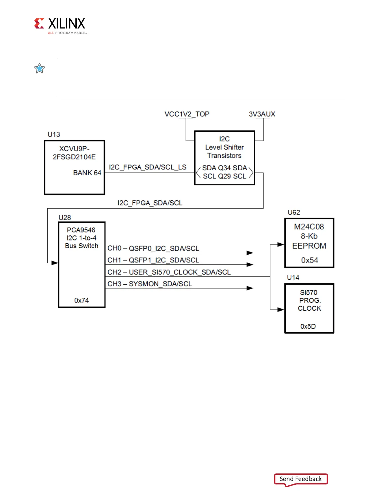
The VCU1525 board I2C_FPGA_SDA/SCL bus topology is shown in Figure 3-13.
IMPORTANT: PCA9546 U28 RESET_B pin 3 is connected to U13 FPGA bank 64 pin BF19 via level-shifter
Q33. PCA9546 U56 RESET_B pin 3 is connected to U19 MPS432 port 6_4 pin 79. The reset nets
I2C_MAIN_RESET_B_LS on U13 FPGA pin BF19 and I2C_MAIN_RESET_B on MSP432 U19 pin 79 net must
both be driven High to enable I2C bus transactions with the devices connected to U28 and U56.
FPGA user applications that communicate with devices on one of the downstream I2C buses
must first set up a path to the desired target bus through the U28 bus switch at I2C address
0x74 (0b1110100).
VCU1525 U28 PCA9546 bus switch hosts both a Si570 programmable clock and an 8-Kbit
M24C08 EEPROM on the USER_SI570_CLOCK_SDA/SCL channel 2 I2C bus.
X-Ref Target - Figure 3-13
Figure 3-13: I2C Bus Topology