Virtex-5 LXT/SXT/FXT FPGA Prototype Platform www.xilinx.com 11
UG229 (v3.0.1) May 21, 2008
Overview
R
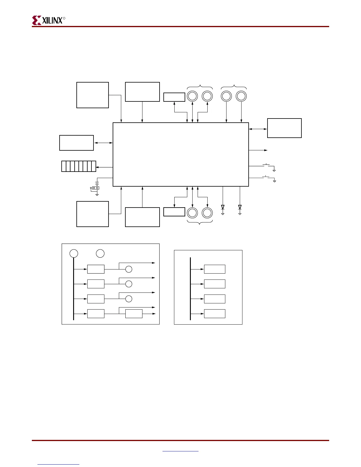
Block Diagram
Figure 1 shows a block diagram of the board.
X-Ref Target - Figure 1
Figure 1: Virtex-5 LXT/SXT/FXT FPGA Prototype Platform Block Diagram
Virtex-5 DUT
Upstream
System ACE
Interface
Connector
User LEDs
UG229_01_051208
DONE
LED
INIT
LED
VBATT
PROGRAM
User RESET
To Test Points
on All Pins
Configuration
Upstream
Interface
Connector
Downstream
Interface
Connector
Downstream
System ACE
Interface
Connector
LVT TL
2x
2x Diff Pair
Clocks
SMA SMA
Power Bus and Switches
5V Jack 5V Brick-or-
VCC Jack
VCCO Jack
VCCAUX Jack
VCCINT
VCCO
VCCAUX
VCC3
VCC1V8
2x
2x Diff Pair
Clocks
SMA
Platfor
m Fl
ash,
SPI, BPI, JTA
G
System
Monitor
SMA
GTP/GTX Transceiver Power Supply
AVCC
VCCO
AVCCPLL
AVTTTX
AVTTRX
The GTP/GTX transceiver power supply names
might have the prefix MGT in other Xilinx
documentation. Names with and without the
MGT prefix are synonymous to each other.
NOTE:
LVT TL
2x Diff Pair
GTP/GTX Clocks
SMA SMA
 Loading...
