Virtex-5 LXT/SXT/FXT FPGA Prototype Platform www.xilinx.com 15
UG229 (v3.0.1) May 21, 2008
Detailed Description
R
AVCCPLL
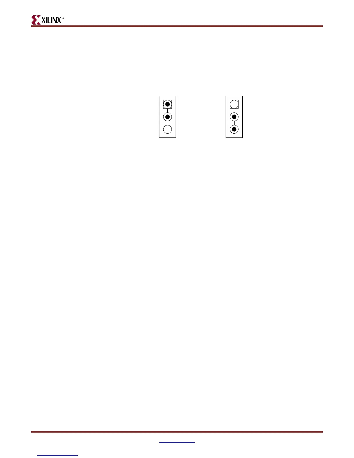
The J84 header adjusts AVCCPLL to 1.2V for LXT/SXT devices and 1.0V for FXT devices
(Figure 3). Header J84 is located directly above header J36 in the upper left quadrant of the
board. However, if your board does not contain header J84, you can ignore Figure 3.
Note:
If your board contains the J84 header, be sure to place a jumper on J84 before powering up
the board for proper operation.
2. Power Supply Jacks
One method of delivering power to the DUT is by way of the power supply jacks: VCCINT
(J33), VCCO (J31), and VCCAUX (J30). See Virtex-5 FPGA Data Sheet: DC and Switching
Characteristics [Ref 1] for the maximum voltage rating for each device. The power supply
jacks are:
• VCCINT
♦ Supplies voltage to the V
CCINT
of the DUT
• VCCO
♦ Supplies I/O voltages to the DUT
♦ Each bank can be powered from one of two sources (V
CCO
, V
CCINT
) by
appropriate placement of jumpers on the header
• VCCAUX
♦ Supplies voltage to the V
CCAUX
DUT pins
X-Ref Target - Figure 3
Figure 3: Power Jumper Setting for LXT, SXT, and FXT Devices
J84
1
3
2
UG229_03_050407
J84
1
3
2
FXT DevicesLXT/SXT Devices
 Loading...
