28 www.xilinx.com Virtex-5 LXT/SXT/FXT FPGA Prototype Platform
UG229 (v3.0.1) May 21, 2008
Detailed Description
R
22. GTP/GTX Transceiver Clocks to SMA
GTP/GTX Transceiver Clock Inputs
The Virtex-5 FPGA prototype platform provides a high-speed differential clock input used
to clock the input and output serial data from the GTP/GTX transceivers. Table 14 shows
GTP/GTX transceiver clocks and their corresponding FPGA pins. The GTP/GTX
transceivers are looped back and are not connected to test points or SMA connectors. See
the Virtex-5 FPGA RocketIO GTP Transceiver User Guide [Ref 4] and the Virtex-5 FPGA
RocketIO GTX Transceiver User Guide [Ref 5] for more information on GTP/GTX transceiver
operation.
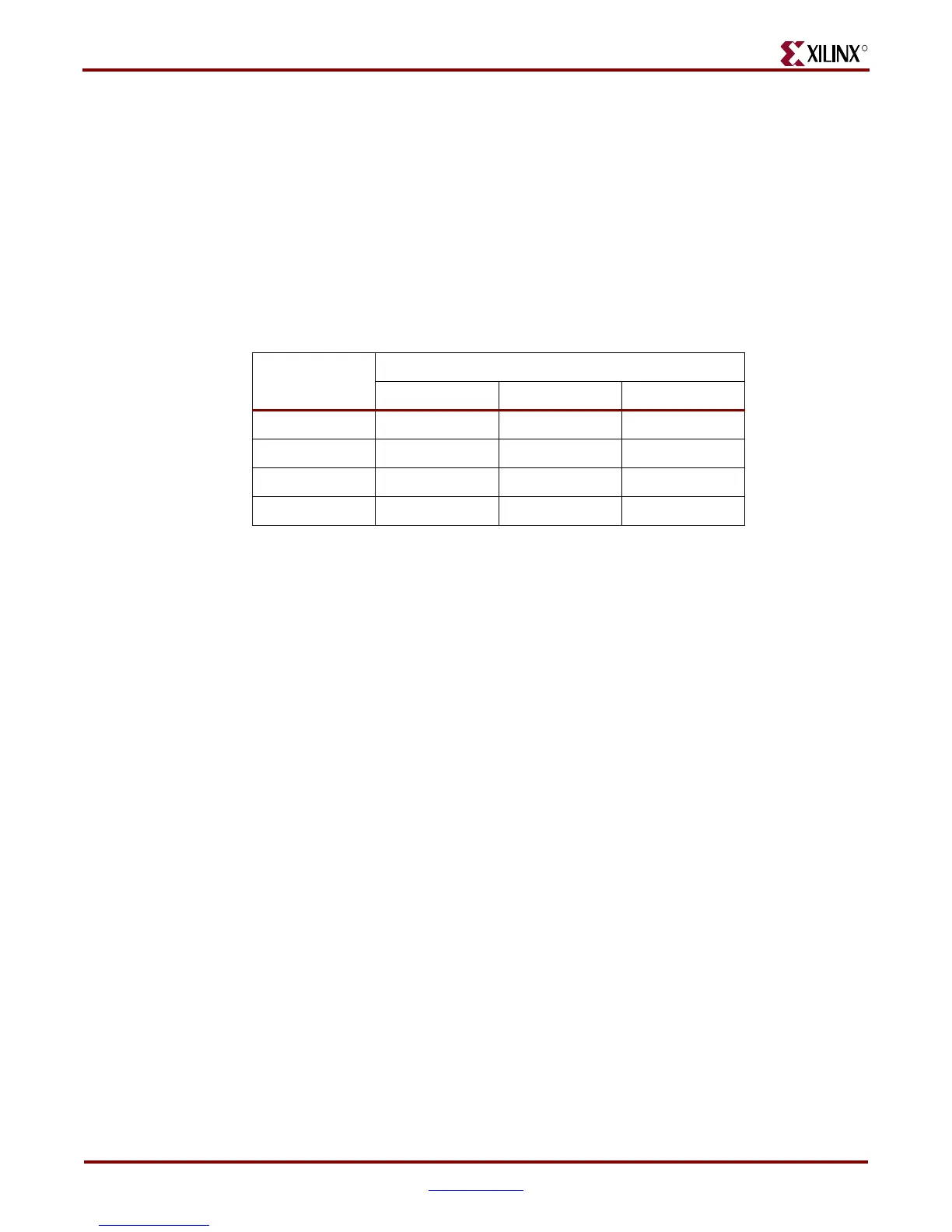
Table 14: GTP/GTX Transceiver Clock Pins
LABEL
Pin Number For Package Type
FF665 FF1136 FF1738
REFCLKN_116 D3 H3 M3
REFCLKP_116 D4 H4 M4
REFCLKN_118 AB3 AF3 AK3
REFCLKP_118 AB4 AF4 AK4
Notes:
1. These GTP/GTX clock pin names might have the prefix MGT in other Xilinx
documentation. Names with and without the MGT prefix are synonymous to
each other.