Virtex-5 LXT/SXT/FXT FPGA Prototype Platform www.xilinx.com 27
UG229 (v3.0.1) May 21, 2008
Detailed Description
R
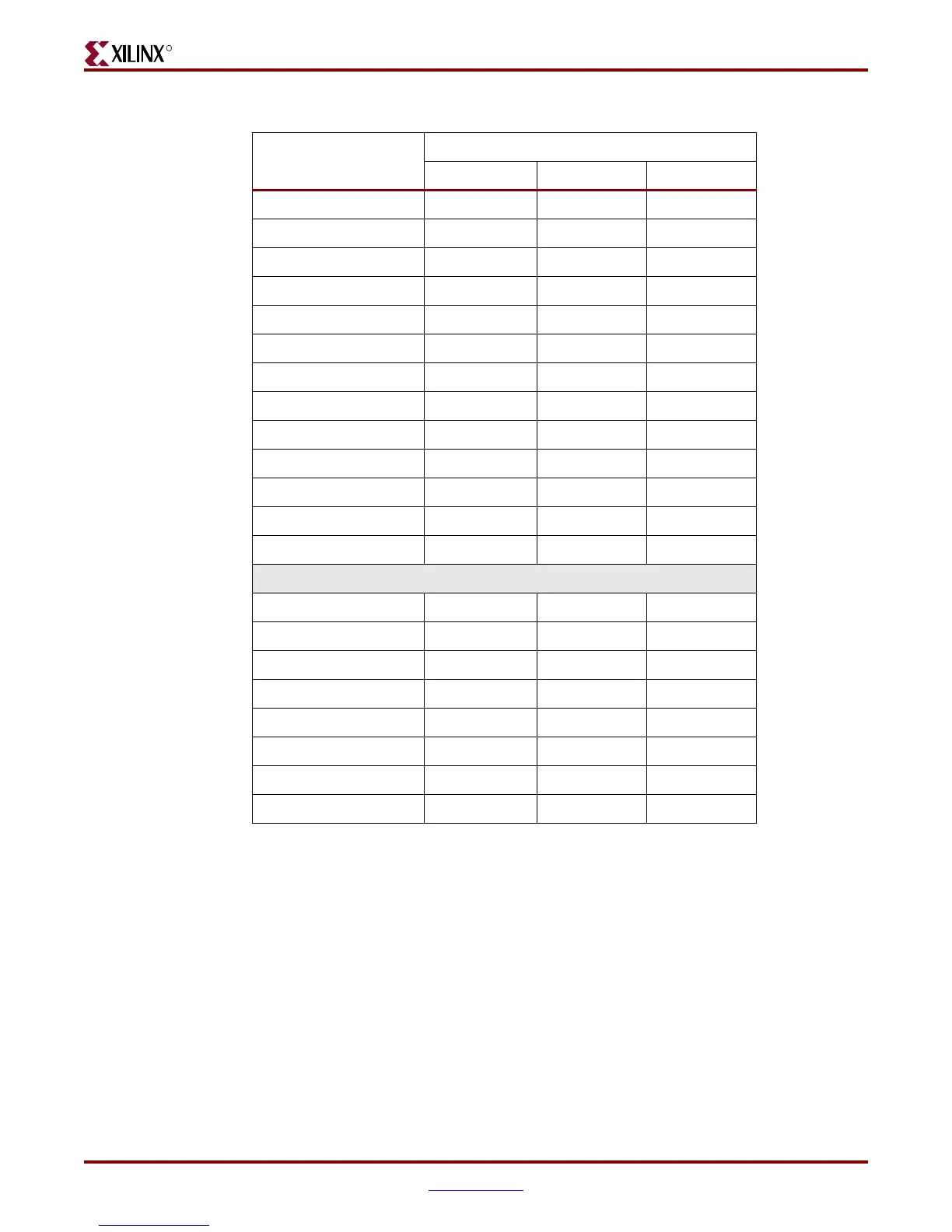
J47 is a three-pin header that allows users to connect the OE signal to V
CC
or to an FPGA
pin. Jumper pin 1 to 2 connects the OE signal to VCC. Jumper pin 2 to 3 connects the OE
signal to an FPGA IOB. Table 13 shows the corresponding FPGA pin.
J54 allows users to connect the revision select (RS) signals to the highest address lines of the
BPI device. Jumper pins 1 to 3 and pins 2 to 4 connect address 23 and address 24 to FPGA
IOBs. Jumper pins 3 to 5 and pins 4 to 6 connect RS0 and RS1 to the highest address lines
of the BPI device. See the Virtex-5 FPGA Configuration User Guide [Ref 3] for more
information on how the RS signals can be applied in a user’s application.
A12 F18 G22 P27
A13 F14 J15 N16
A14 F15 K16 M16
A15 F17 K21 N26
A16 G17 J22 P26
A17 G14 L16 P17
A18 H13 L15 P18
A19 G16 L20 P25
A20 G15 L21 N25
A21 Y18 AE23 AM29
A22 AA18 AE22 AL30
A23 Y11 AG12 AK14
A24 AA10 AF13 AK15
WE_N AA17 AF20 AM28
WP_N Y5 M5 AA6
ADV_N Y6 M6 AA7
RST_N K7 U7 N6
CE_N Y12 AE14 AL14
WAIT K6 T8 N5
CLK U5 J7 U6
OE_N AA12 AF14 AM13
Table 13: BPI Pins (Cont’d)
Label
Pin Number For Package Type
FF665 FF1136 FF1738