Virtex-5 LXT/SXT/FXT FPGA Prototype Platform www.xilinx.com 29
UG229 (v3.0.1) May 21, 2008
Detailed Description
R
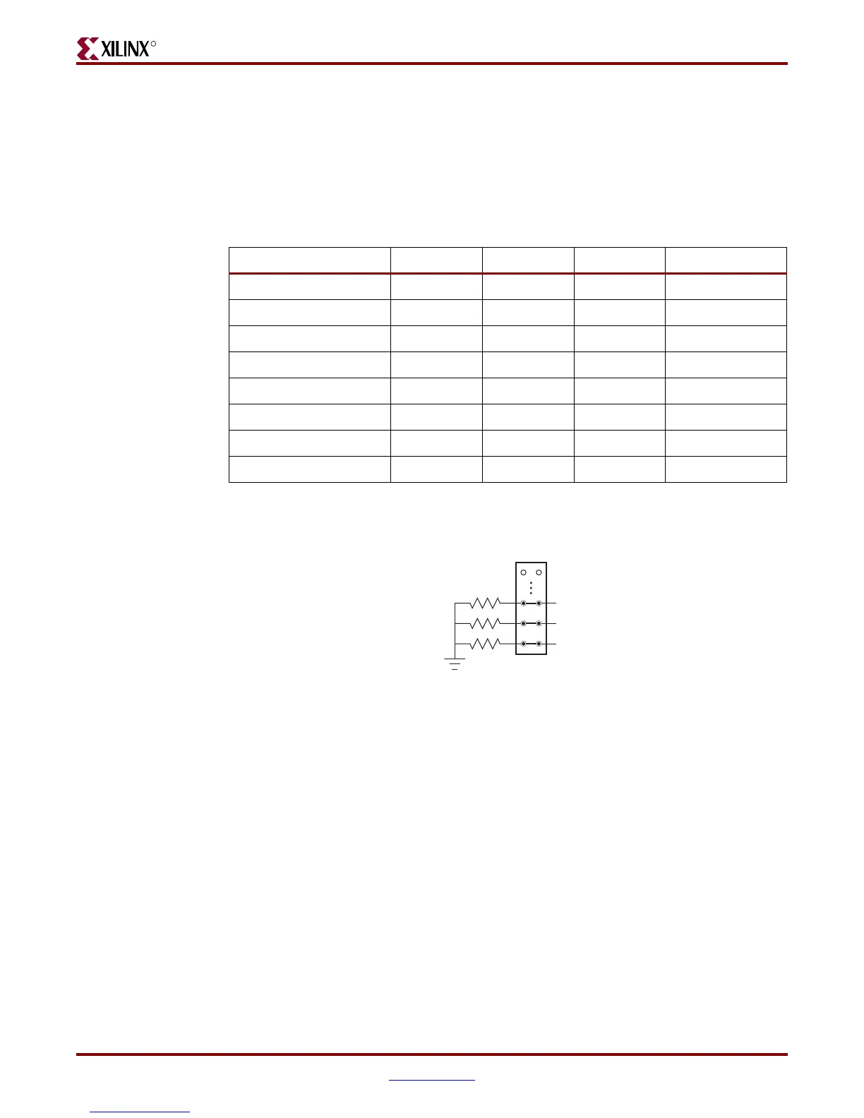
23. Configuration Mode Pins
The three jumpers on J17 control the configuration mode pins M0-M2. These pins set the
configuration mode for the FPGA and determine the direction of CCLK (Table 15 and
Figure 9). A jumper across both columns of J17 for each mode pin sets logic 0; removing
the jumper sets logic 1. The default value 000 corresponds to the Master Serial
configuration mode.
Table 15: Configuration Mode Pin Jumper Settings
Configuration Mode M2 M1 M0 CCLK Direction
Master Serial 0 0 0 Output
Master SPI 0 0 1 Output
Master BPI-Up 0 1 0 Output
Master BPI-Down 0 1 1 Output
Master SelectMAP 1 0 0 Output
JTAG 1 0 1 Input (TCK)
Slave SelectMAP 1 1 0 Input
Slave Serial 1 1 1 Input
X-Ref Target - Figure 9
Figure 9: Default Configuration Mode Jumper Settings
UG229_09_041108
J17
M2
M1
M0
(HDR_2x29)