Virtex-6 FPGA Connectivity Kit Getting Started www.xilinx.com 11
UG664 (v1.4) July 6, 2011
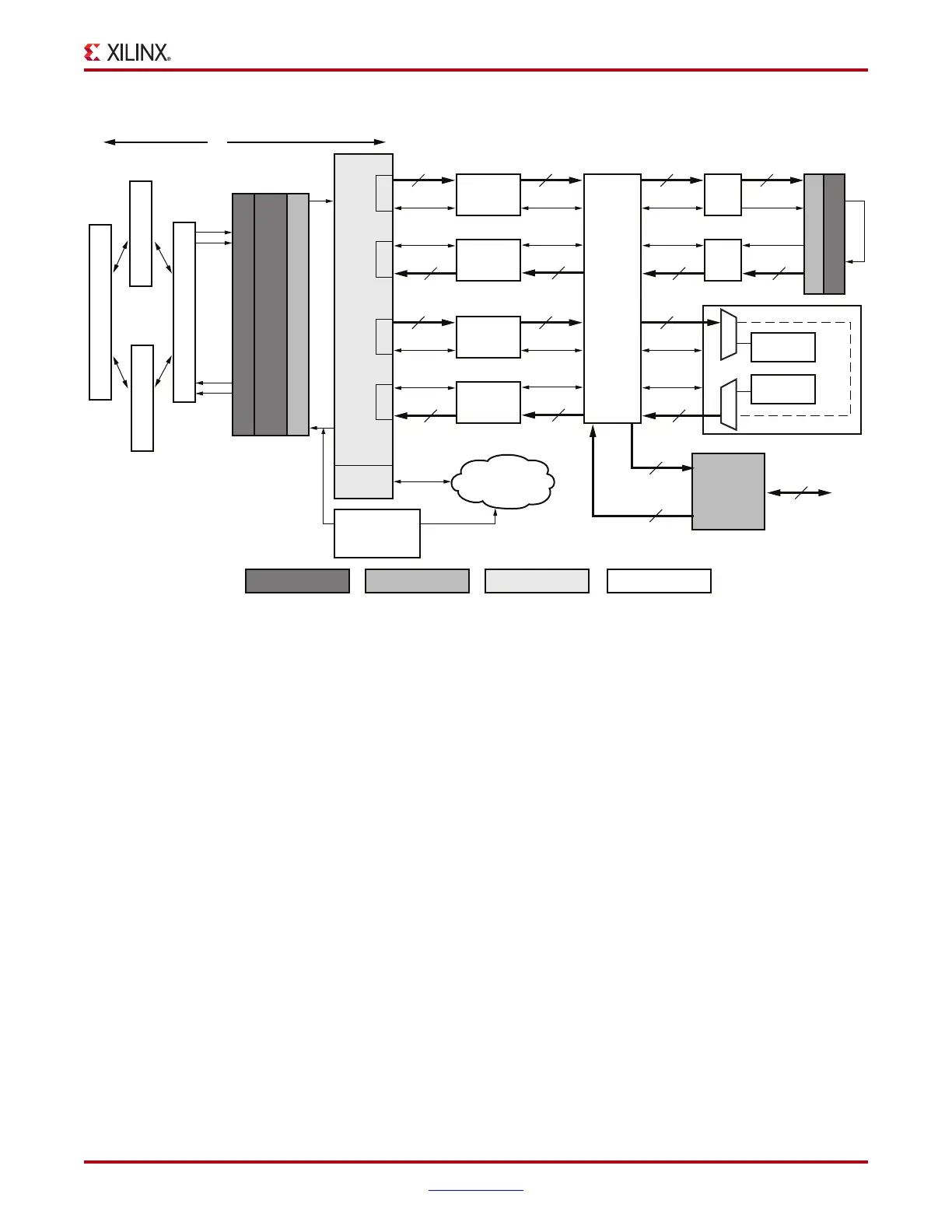
Getting Started with the Connectivity Targeted Reference Design Demo
The Virtex-6 FPGA Connectivity TRD features these components:
• Virtex-6 FPGA Integrated Block for PCI Express core configured as a
4-lane at 5 Gb/s or 8-lane at 2.5 Gb/s Endpoint for PCI Express, v2.0
• A performance monitor tracks the PCIe® data bandwidth by measuring data bus
utilization on:
• AXI4-Stream interface
• Packet DMA for PCI Express from Northwest Logic, a multichannel DMA that:
• Supports full-duplex operation with independent transmit and receive paths
• Provides a packetized interface on the backend similar to LocalLink
• Monitors data transfers in the receive and transmit directions
• Provides a control plane interface to access user-defined registers
• Multiport Virtual FIFO
• The Memory Interface Controller is delivered through the Virtex-6 FPGA Memory
Interface Generator (MIG) tool.
• The virtual FIFO is a highly efficient layer around the native interface of the
Virtex-6 FPGA Memory Controller and an external DDR3 memory device.
• XAUI LogiCORE IP that utilizes serial I/O transceivers to provide a throughput of up
to 10 Gb/s
XAUI TX and XAUI RX blocks align data as per the XGMII format.
• Control logic to interface between the DMA and the multiport Virtual FIFO.
X-Ref Target - Figure 1
Figure 1: Block Diagram of the Virtex-6 FPGA Targeted Reference Design
Packet
DMA
Software Hardware
C2S
S2C
C2S
S2C
x4 PCIe Link @ 5.0 Gb/s or
x8 PCIe Link @ 2.5 Gb/s
Third Party IP FPGA Logic
64-bit AXI4-Stream Interface @ 250 MHz
Register
Interface
Performance
Monitor
User Space
Registers
Packet
Control
with CRC
S2C_Ctrl
S2C_Data
64
GTX Transceivers
x4 @ 5 Gb/s / x8 @ 2.5 Gb/s
Integrated Block for PCI Express, v2.0
Wrapper for PCI Express
Base DMA Driver
Raw Data Driver
XAUI Driver
GUI
Xilinx IPIntegrated Blocks
Native
Interface
of DDR3
Memory
Controller
Multiport
Virtual
FIFO
UG664_01_092810
Control
WR_Data
64
C2S_Ctrl
C2S_Data
64
XGMII
TX
XAUI
GTX Transceivers
Control
RD_Data
64
Control
Data
64
XGMII
RX
Control
WR_Data
64
Control
Data
64
@400 MHz
@200 MHz
@250 MHz
@156.25 MHz@250 MHz@250 MHz
@250 MHz@250 MHz
@156.25 MHz
DDR3
64
Control
RD_Data
64
Control
Control
S2C_Ctrl
S2C_Data
64
Control
WR_Data
64
C2S_Ctrl
C2S_Data
64
Raw Data
Loopback
Control
RD_Data
64
Control
WR_Data
64
256
256
Control
RD_Data
64
Packet
Control
with CRC
Generator
Checker

 Loading...

