58 www.xilinx.com Virtex-6 FPGA Connectivity Kit Getting Started
UG664 (v1.4) July 6, 2011
Next Steps
PCI Express
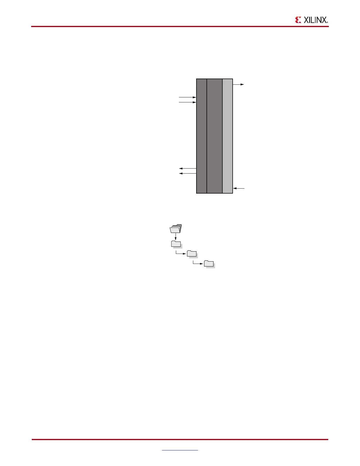
Figure 52 shows the design module for PCI Express. Figure 53 shows the design file
structure.
X-Ref Target - Figure 52
Figure 52: Design Module for PCI Express
X-Ref Target - Figure 53
Figure 53: Design FIles for PCI Express
x4 PCIe Link @ 5.0 Gb/s or
x8 PCIe Link @ 2.5 Gb/s
64-bit AXI4-Stream Interface @ 250 MHz
GTX Transceivers
x4 @ 5 Gb/s / x8 @ 2.5 Gb/s
Integrated Block for PCI Express, v2.0
Wrapper for PCI Express
UG664_16_051911
UG664_17_090
810
v6_pcie_10Gdma_ddr3_xaui_axi
design
ip_cores
pcie

 Loading...

