Virtex-6 FPGA Connectivity Kit Getting Started www.xilinx.com 57
UG664 (v1.4) July 6, 2011
Next Steps
Next Steps
Connectivity TRD Modules
This section outlines the correlation between the design modules and corresponding
design source files for the various blocks of the design. Refer to Figure 1, page 11 for the
detailed block diagram of the Virtex-6 FPGA Connectivity TRD. Table 1 shows the design
file organization per module.
For functional details on these modules, refer to the “Functional Description” chapter in
UG379
, Virtex-6 FPGA Connectivity Targeted Reference Design with AXI4 Protocol User Guide.
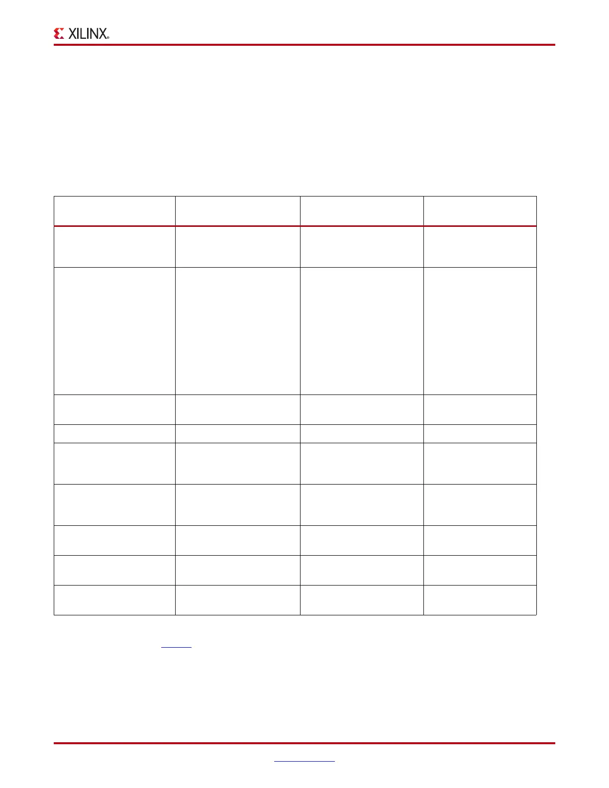
Table 1: Design File Organization for the Virtex-6 FPGA Connectivity TRD
Module Name Source Files/Directories LogiCORE IP
Connectivity TRD
Source
Top-Level Module:
Virtex-6 FPGA
Connectivity TRD
v6_pcie_10Gdma_ddr3_
xaui_axi
✓
PCI Express (x4) pcie
✓
(Endpoint for PCI Express
core with AXI4-Stream
interface - CORE generator
output)
OR
(Endpoint for PCI Express
core with transaction
interface - CORE generator
output)
Packet DMA dma
Netlist deliverable only
(from Northwest Logic)
Multiport Virtual FIFO virtual_fifo ✓
Memory Controller Block mig
✓
(MIG - CORE Generator
output)
XAUI xaui
✓
(XAUI core -
CORE Generator output)
Clocking, Reset, Register
Interface
reset_control,
registers
✓
Software Device Driver
linux_driver,
windows_driver
✓
Software Application/GUI
linux_driver/xpmon,
windows_driver/xpmon
✓

 Loading...

