Virtex-6 FPGA Connectivity Kit Getting Started www.xilinx.com 59
UG664 (v1.4) July 6, 2011
Next Steps
Packet DMA
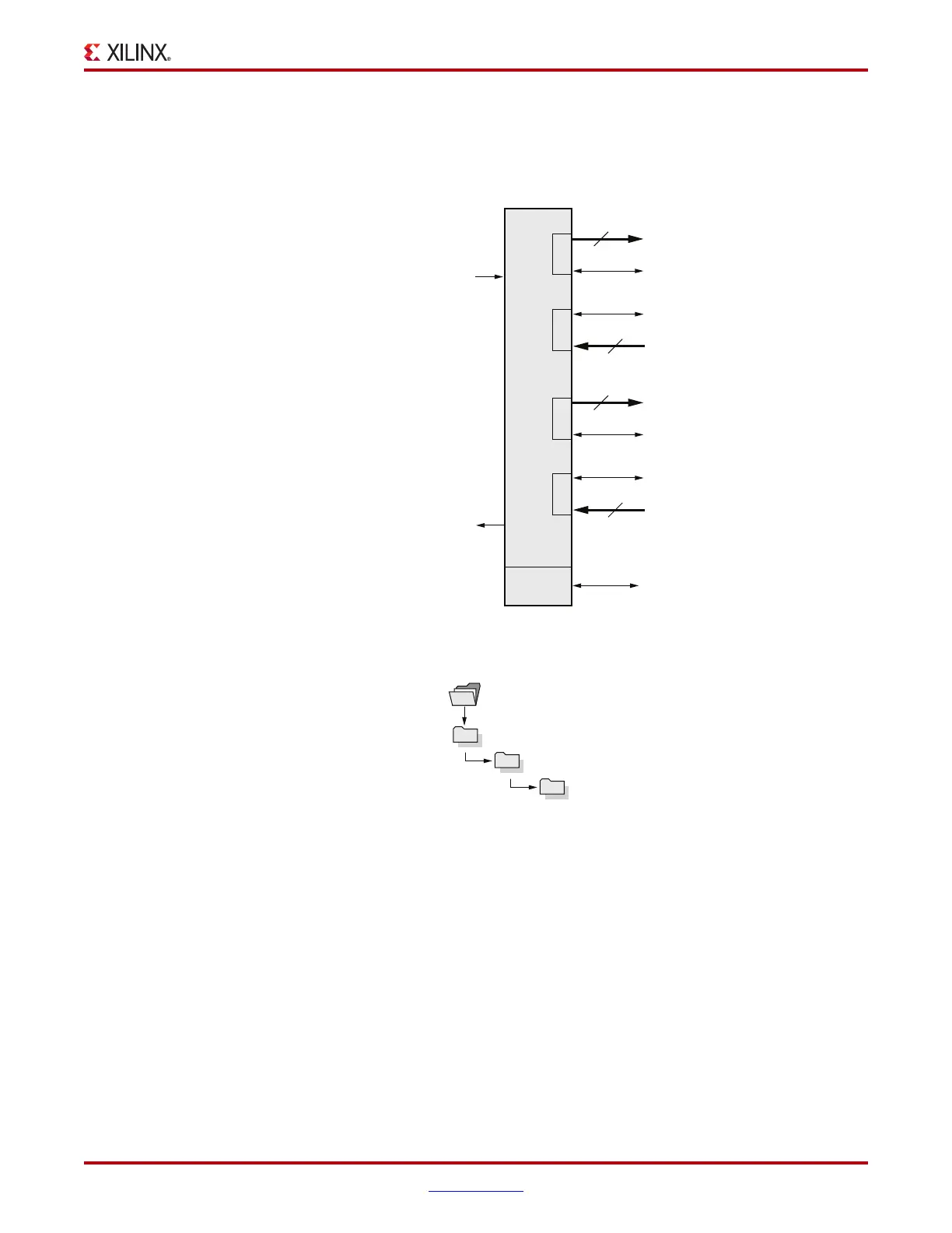
Figure 54 shows the design module for Packet DMA. Figure 55 shows the design file
structure.
X-Ref Target - Figure 54
Figure 54: Packet DMA Design Module
X-Ref Target - Figure 55
Figure 55: Packet DMA Design FIles
UG664_18_051911
Packet
DMA
C2S
S2C
C2S
S2C
64-bit AXI4-Stream Basic Interface @ 250 MHz
Register
Interface
S2C_Ctrl
S2C_Data
64
C2S_Ctrl
C2S_Data
@250 MHz
@250 MHz
S2C_Ctrl
S2C_Data
64
C2S_Ctrl
C2S_Data
UG664_19_090810
v6_pcie_10Gdma_ddr3_xaui_axi
design
ip_cores
dma

 Loading...

