60 www.xilinx.com Virtex-6 FPGA Connectivity Kit Getting Started
UG664 (v1.4) July 6, 2011
Next Steps
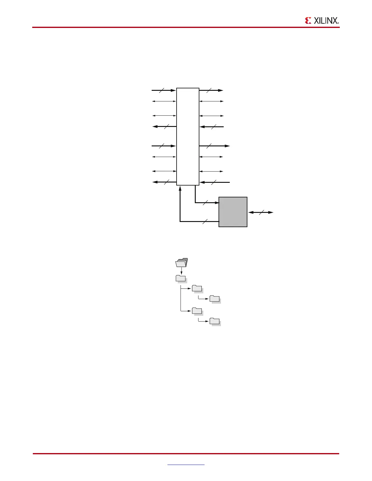
Multiport Virtual FIFO and Memory Controller Block
Figure 56 shows the design module for the multiport virtual FIFO and memory controller
block. Figure 57 shows the design file structure.
X-Ref Target - Figure 56
Figure 56: Multiport Virtual FIFO and Memory Controller Block Design Module
X-Ref Target - Figure 57
Figure 57: Multiport Virtual FIFO and Memory Controller Design FIles
UG664_20_060110
Native
Interface
of DDR3
Memory
Controller
Multiport
Virtual
FIFO
Control
WR_Data
Control
RD_Data
6464
Control
WR_Data
64
@400 MHz
@200 MHz
@250 MHz
@156.25 MHz@250 MHz
@250 MHz
DDR3
64
256
256
Control
RD_Data
64
Control
WR_Data
Control
RD_Data
6464
Control
WR_Data
64
Control
RD_Data
64
UG664_21_090810
v6_pcie_10Gdma_ddr3_xaui_axi
design
source
virtual_fifo
ip_cores
mig

 Loading...

