Do you have a question about the Yaesu FTDX3000 and is the answer not in the manual?
| Antenna Impedance | 50 Ohms |
|---|---|
| Type | HF/50 MHz Transceiver |
| Supply Voltage | 13.8 V DC ±15% |
| Antenna Connector | SO-239 |
| IF DSP | Yes |
| Modes | AM, FM, RTTY |
| Receiver Type | Triple Conversion Superheterodyne |
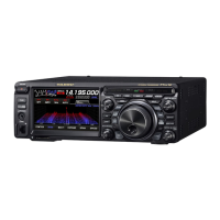
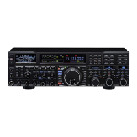
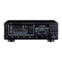
| Display | 4.3-inch TFT Full-Color |
Shows the external parts and their assembly.
Illustrates front panel and display assembly components.
Details chassis and shield plate components.
Depicts internal main chassis and unit placements.
Shows internal component layout and shielding.
Illustrates internal board unit assembly.
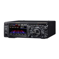
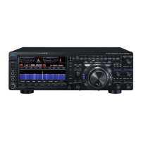
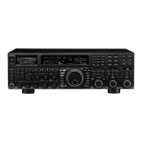
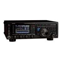
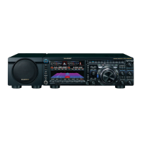
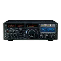
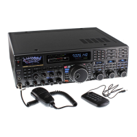
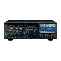
Lists general operating parameters and physical characteristics.
Details transmitter output power and modulation types.
Covers receiver circuit type and sensitivity specifications.
Provides a high-level system overview with functional blocks.
Illustrates internal signal and power connections between units.
Covers essential safety and preparatory steps before alignment.
Lists necessary tools and instruments for alignment procedures.
Details critical setup and environmental considerations for accurate alignment.
Describes voltage adjustments on the PA Unit for proper operation.
Details calibration for temperature compensation and fan control.
Covers alignment of IF shift and bandwidth controls.
Describes adjustments for the compressor meter readings.
Details alignment of local oscillator circuits for frequency accuracy.
Covers voltage adjustments for Voltage Controlled Oscillators.
Describes alignment of the reference oscillator frequency.
Details adjustments for the 1st local oscillator across frequency bands.
Covers adjustments for the 2nd local oscillator level.
Details alignment of IF transformers for optimal signal processing.
Describes adjustments for the 14.200 MHz MCF circuit.
Covers MCF adjustments for 14.200 MHz with different filters.
Details alignment of IF traps to minimize unwanted signals.
Covers alignment of the noise blanker circuit.
Details adjustments for the Automatic Gain Control circuit.
Covers alignment of IF gain stages across frequency bands.
Describes calibration of the S-meter readings.
Covers gain adjustments for FM mode operation.
Details transmitter adjustments including TX IFT.
Covers alignment of the Transmit Intermediate Frequency Transformer.
Details adjustments for the Power Amplifier unit.
Describes idling current adjustments for the pre-drive stage.
Covers idling current adjustments for the drive stage.
Details idling current adjustments for the final power stage.
Covers balance adjustment for the antenna tuner coupler.
Describes automatic level control adjustments across amateur bands.
Details alignment of the ALC meter for proper power control.
Covers reverse ALC adjustments for different frequency bands.
Details alignment of FM deviation for transmitter output.
Describes calibration of the Standing Wave Ratio meter.
Covers adjustments for the Internal DC Deviation meter.
Shows the schematic for the main unit's circuitry.
Provides the schematic for the Band Pass Filter unit.
Shows the schematic for the SCP unit.
Provides the schematic for the control unit.
Shows the schematic for the local oscillator unit.
Provides the schematic for the power amplifier unit.
Shows the schematic for the digital signal processing unit.
Provides the schematic for the FFT unit.
Shows the schematic for the first display unit.
Provides the schematic for the second display unit.
Shows the schematic for the SW-A unit.
Provides the schematic for the SW-B unit.
Shows the schematic for the VR-A unit.
Provides the schematic for the jack unit.
Shows the schematic for the microphone unit.
Lists all components for the main unit with reference numbers.