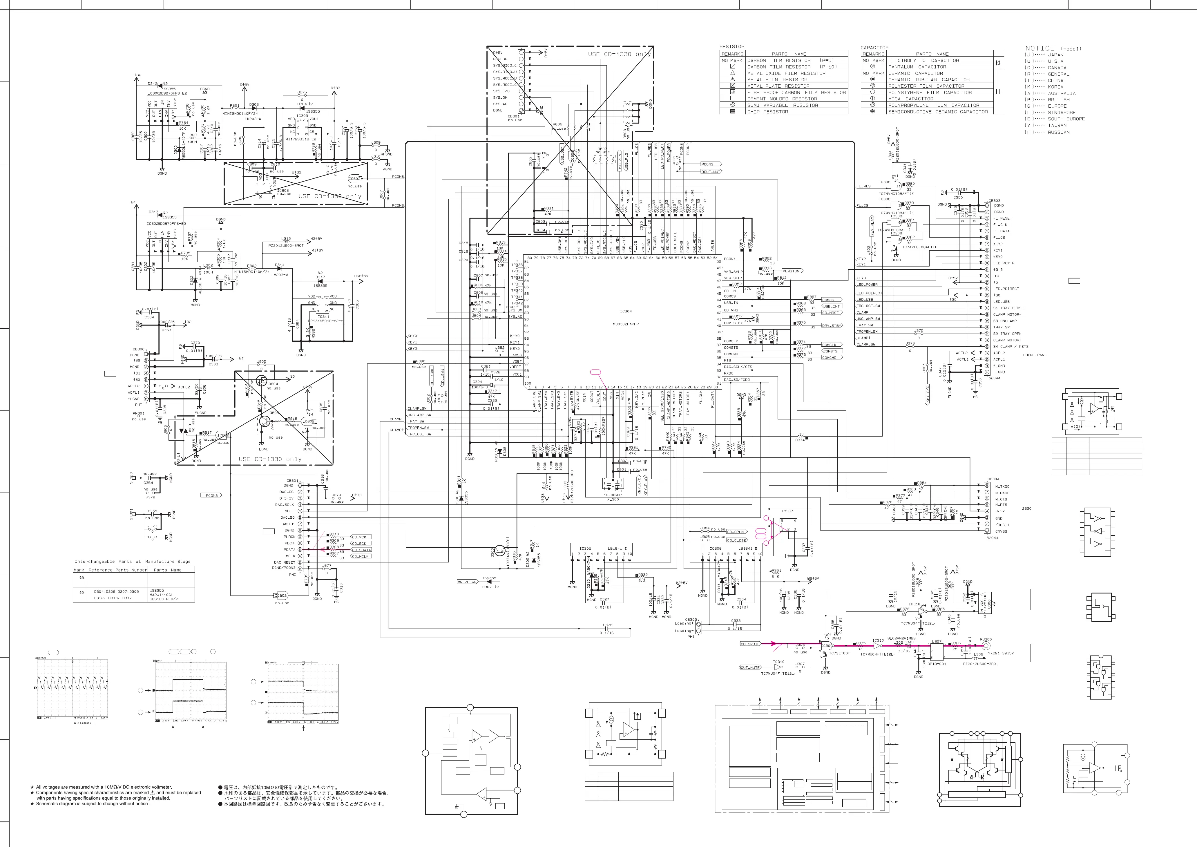
IC304
IC305
CB301
CB300
IC311
IC302
IC300
IC303
IC306
IC307
IC309
IC310
IC310
CB304
CB303
IC308
IC308
IC308
IC308
IC310
A
1
2
3
4
5
6
7
8
9
10
BCDEFGH I JK
L MN
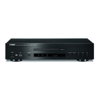
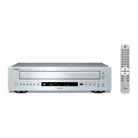
CD-S700
40
DIGITAL 2/2
A-3
B-2
B-1
4.9
4.2
4.9
4.9
3.3
3.3
0
4.2
4.2
0
4.2
0
20.0
20.0
4.9
0
1.0
10.0
7.9
7.9
7.9
7.4
7.4
0
0
7.4
0
0
0
3.3
3.3
0
1.7
4.9
1.7
0
3.3
3.3
3.3
3.3
3.3
3.3
0
0
7.9
7.9
0.6
0.8
0.8
0
1.0
0
0.4
0.6
0
0
0
7.9
7.9
0.6
3.3
3.3
0
0.8
0.8
0.6
0
3.1
3.3
3.3
0
0
3.3
3.3
3.3
0
0
3.3
3.3
4.9
4.9
4.9
0
3.3
0
4.9
0
0
0
3.3
3.3
3.3
3.3
0
0
0
3.3
1.7
0
1.5
3.3
3.3
3.3
0
0
0
0
3.3
0
3.3
3.3
3.3
3.3
0
0
3.3
0
0
0
3.2
3.2
3.3
3.3
3.3
3.3
0
1.6
3.3
3.3
0
3.3
3.3
3.3
0
0
0
3.3
3.3
0
4.9
0
2.5
2.5
0
2.5
5.0
2.5
2.5
0
5.0
2.5
0
20.0
20.0
7.9
0
1.1
20.0
1
2
DIGITAL OUT
AUDIO OUT
C816
BD5229G–TR
J812
J810
C817
2200P(B)
MICROPROCESSOR
CLAMP DRIVER
LOADING DRIVER
BUFFER AMP.
LEVEL
SHIFTER
OPTICAL
COAXIAL
DIGITAL OUT
Vref
Vout
GND
V
DD
N.C.
N.C.
4
1
2
3
5
–
+
IC307: BD4829G-TR
Voltage detector IC
IC305, 306: LB1641
Motor driver
INPUT LOGIC
IN 1
IN 2
VZ
P1
P2
OUT 1
OUT 2
VCC 2
VCC 1
GND
PRE DRIVER
1
3281097
4
6
5
IC304: M30302FAPFP
Single-chip 16-bit microprocessor
Timer (16-bit)
Peripheral function
Input (timer A) x3
Output (timer B) x3
Watchdog timer
(15-bit)
DMAC
(2-channel)
A/D converter
(10-bit
X
18-channel
)
System clock generator
X
IN
-X
OUT
X
CIN
-X
COUT
M16C/60 series
Microprocessor core
Port P0
8
Port P1
8
Port P2
8
Port P3
8
Port P4
8
Port P5
8
Port P6
8
8
R0LR0H
R1H R1L
R2
R3
ISP
USP
INTB
SB
CRC arithmetic circuit (CCITT)
(Polynomial : X
16
+X
12
+X
5
+1)
Multiplier
7
8
Port P9
8
Port P10
Port P8_5
Port P8
Port P7
Memory
ROM
(Note 1)
RAM
(Note 2)
FB
A1
FB
A1
A0
FLG
PC
UART or clock synchronous type
serial I/O
(3-channel)
Note 1: ROM contents vary depending on types.
RAM contents vary depending on types.
Note 2:
VDD
CE
Pin No.
1
2, 5
3
4
6
Symbol
V
OUT
GND
CE
NC
V
DD
Description
Output Pin of Voltage Regulator
Ground Pin
Chip Enable Pin
No Connection
Input Pin
Vref
61
3 2,5
Current Limit
VOUT
GND
IC303: R1172S331B-E2-F
CMOS-based positive-voltage regulator IC
IC308: TC74VHCT08AFT
Quad 2-input AND gate
Vcc14
4B
4A
4Y
3B
3A
3Y
1A 1
2
3
13
12
11
10
9
8
4
5
6
7
1B
1Y
2A
2B
2Y
GND
1
3
2
5
4
GND
V
CC
IC309: TS7ST00F
2-input NAND gate
IN A
IN B
OUT Y
IC310: TC7WU04F
Triple inverter
1
2
3
4
8
7
6
5
1A
3Y
2A
GND
V
CC
1Y
3A
2Y
VDD
CE
Pin No.
1
2
3
4
5
6
Symbol
V
OUT
GND
CE
NC
V
DD
Description
Output Pin of Voltage Regulator
Ground Pin
GND Ground Pin
Chip Enable Pin (“H” Active)
No Connection
Input Pin
Vref
16
2,54
Current Limit
VOUT
GND
IC311: RP131S501D-E2-F
Voltage regulator
POINT B-1 B-2 1 / Pin2, 2 / Pin1 of IC307
12 pin
1 pin
2 pin
1 pin
2
1
2
AC cable ON AC cable OFF AC cable OFF
POINT A-3 XL300 (Pin 13 of IC304)
OSC
PWM COMP DRIVER
STBY
STBY
OUT
INV
GND
VCC
TSD
OCP
Error AMP
SS
CTL
LOGIC
IC300, 302: BD9870FPS-E2
High stand voltage 1 channel step-down switching regulator
VREF
1
5
FIN
4
2
to OPERATION (4)_W208
Page 42
L5
to OPERATION (3)_W2
Page 41
G6
to OPERATION (9)_CB151
Writing port
Page 42
F8
To Loader ass’y
 Loading...