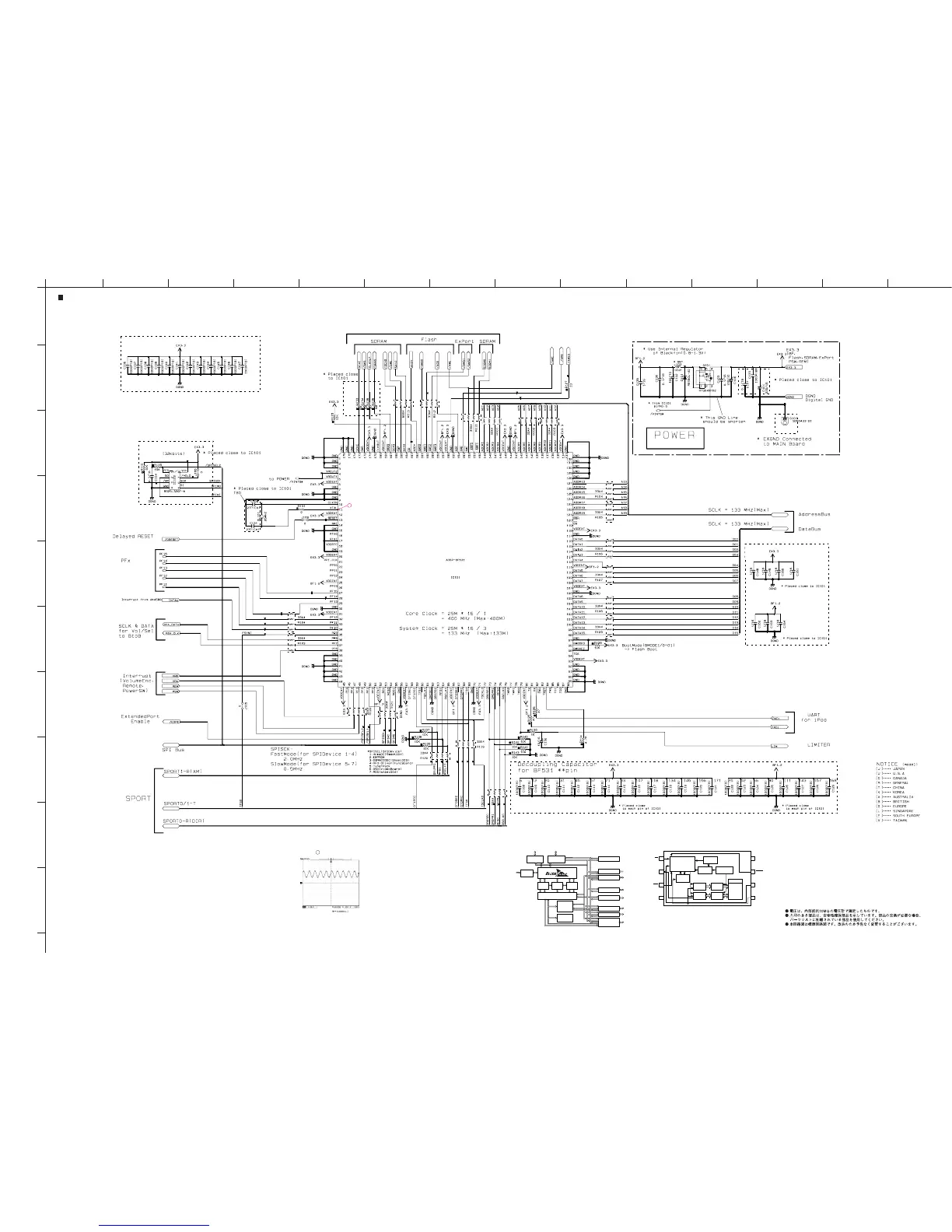
IC101
IC102
A
1
2
3
4
5
6
7
8
9
10
BCDEFGH I JK
L MN
RX-V361/HTR-6030/DSP-AX361
71
★ All voltages are measured with a 10MΩ/V DC electronic voltmeter.
★ Components having special characteristics are marked s and must be replaced
with parts having specifications equal to those originally installed.
★ Schematic diagram is subject to change without notice.
DSP 1/5
SCHEMATIC DIAGRAMS
3.4
3.4
0
0
3.4
3.3
3.3
0.1
3.4
3.4
0.1
1.4
3.4
0.4
3.4
0
3.4
0.8
1.7
2.2
0
0.4
0.2
0.4
1.4
0.1
2.6
1.7
0
3.4
2.2
1.9
1.1
2.2
2.2
3.2
1.4
0
0
0.2
0
0
0
0
0
0
0
3.4
2.3
3.4
0
1.8
1.4
3.3
2.6
3.1
0.8
3.3
0.1
3.3
3.3
3.4
3.4
1.4
3.4
0
3.4
3.4
3.4
3.4
0.2
1.4
3.3
2.1
2.0
3.4
0
1.4
1.8
1.8
1.8
1.8
1.9
1.7
1.1
1.0
3.4
0
0
0
0
0
1.4
1.4
1.4
3.4
2.0
0
0
0
0
2.2
0.2
0.2
0.2
0.1
0.1
0.1
3.4
0
0.2
0.3
0.3
0.3
0.3
1.4
0.3
0.3
0.3
3.4
0
1.6
1.6
1.6
1.6
1.6
1.6
1.6
1.6
0
3.4
0
0
3.3
0
0
0
0
2.0
2.0
3.4
0
0
0
1.7
1.7
3.4
3.3
0
0
0
0
3.4
1.4
3.4
3.4
0.1
0
3.4
0.1
0.2
3.3
2.2
0.1
0.1
3.4
0
0
0
0
0
0
3.4
3.4
3.4
0.3
3.4
0
3
POINT 3 Pin 11 of IC101
to DSP 2/5
to DSP 5/5
to DSP 2/5
to DSP 5/5
to DSP 5/5
to DSP 5/5
to DSP 3/5, 4/5
to DSP 4/5
to DSP3/5
to DSP 2/5
to DSP 5/5
to DSP 5/5
to DSP 3/5
MICROPROCESSOR
EEPROM
IC101: ADSP-BF531 CPU
Microprocessor
IC102: BR25L320F-W EEPROM
SPI BUS 32 k-bit (4,096 x 8-bit) EEPROM
1
CS
INSTRUCTION DECODE
CONTROL CLOCK
GENERATION
INSTRUCTION
REGISTER
2
SO
3
WP
4
GND
8
Vcc
7
HOLD
6
SCK
5
SI
VOLTAGE
DETECTION
WRITE
INHIBITION
ADDRESS
REGISTER
DATA
REGISTER
8bit
READ/WRITE
AMP
32,768bit
EEPROM
STATUS REGISTER
ADDRESS
DECODER
HIGH VOLTAGE
GENERATOR
8bit
12bit
12bit
PPI/GPIO
L1 data
memory
JTAG test
and emulation
Voltage
regulator
L1 order
memory
Memory
management
unit
Core/System bus interface
Real time clock
UART port IrDA®
Serial port (2)
DMA controller
Boot ROM
SPI port
External port for flash
and SDRAM control
Event controller/
Core timer
Watch dock timer
Timer0, Timer1, Timer2
 Loading...