CB261
CB202
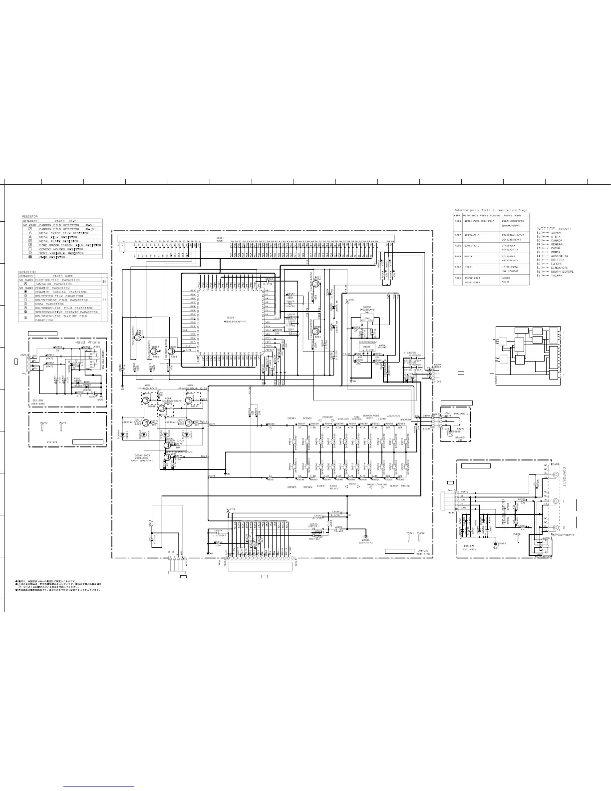
IC201
W2004
W2003
CB203
CB204 CB274
W2351
A
1
2
3
4
5
6
7
8
9
10
BCDEFGH I JK
L MN
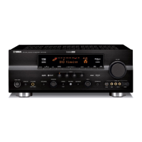
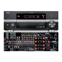
RX-V361/HTR-6030/DSP-AX361
76
★ All voltages are measured with a 10MΩ/V DC electronic voltmeter.
★ Components having special characteristics are marked s and must be replaced
with parts having specifications equal to those originally installed.
★ Schematic diagram is subject to change without notice.
OPERATION 1/2
3.2
3.2
3.2
3.2
3.2
0
0
3.2
3.2
3.2
1.9
1.9
0.4 1.1
0
1.9
3.2
3.2
0
0
0
0
1.9
0
1.9
0
0
0
-24.9
-24.9
-21.6
-19.3
-19.3
-25.0
-25.0
-25.0
-25.0
-25.0
-25.0
-25.0
-25.0
-25.0
-25.0
-25.0
-25.0
-25.0
-25.0
-24.9
-24.9
-24.9
-26.6
-24.9
-21.6
-15.1
-16.8
-15.1
-21.6
-20.0
-23.3
-24.9
-24.9
-13.4
-21.6
-24.9
-21.6
-21.6
-13.5
-20.0
-21.7
-18.4
-21.7
-13.5
-18.4
-24.9
-23.2
-23.3
-13.5
-16.7
-26.6
-26.0
-24.9
-24.9
-13.5
-23.3
-13.5
-15.2
-18.4
-19.3
-19.3
-25.0
-25.0
-25.0
-25.0
-25.0
-25.0
-25.0
-25.0
-25.0
-25.0
-25.0
-25.0
-25.0
-25.0
-25.0
-26.8
-21.6
-13.5
-20.0
-21.7
-18.4
-21.7
-13.5
-18.4
-24.9
-23.2
-23.3
-13.5
-16.7
3.2
-26.6
-26.0
3.2
-18.4
3.2
-18.4
-18.4
-18.4
-19.3
-23.3
3.2
0
0
0
0
0
0
0
0
3.2
-26.8
-24.9
-24.9
-13.5
-23.3
-13.5
-15.2
-18.4
3.2
1.5
1.5
0
3.2
3.2
3.2
3.2
-21.6
-13.4
-24.9
-24.9
-23.3
-20.0
-21.6
-15.1
-16.8
-15.1
-21.6
-24.9
-26.6
-24.9
-25.0
-24.9
3.2
-24.9
-25.0
3.2
-24.9
-25.0
0
0
0
0
0
52
Display
controller
Serial
receive
circuit
Digit
output
circuit
Clock
generator
DIG11/
SEG42
51
DIG12/
SEG41
50
DIG13/
SEG40
49
DIG14/
SEG39
48
DIG15/
SEG38
47
DIG16/
SEG37
46
DIG17/
SEG36
45
SEG35
XOUT
6
Vcc1
8
Vcc2
18
Vss
5
Vp
64
XIN
7
CS
SCK
3
SDATA
4
RESET
1
SEG00
44
9
SEG34
SEG26
17
19
SEG25
Segment
output
circuit
Display code
RAM
(8-bit x 60)
CGROM
(35 bit x 166)
CGROM
(35 bit x 16)
code
select
Code
write
Code/
command
control
circuit
DIG00
63
53
DIG10
2
data
timing
clock
dot data
write
scan pulse
Segment/
Digit
select/
output
circuit
IC201: M66003-0131FP-R
18 digit 5 x 7 segment VFD controller/driver
OPERATION (1)
OPERATION (7)
OPERATION (11)
OPERATION (10)
OPERATION (6)
VFD
VIDEO
AUDIO
PORTABLE
to MAIN (1)_W103
Page 78
I4
to DSP_CB408
Page 74
C7
to MAIN (4)_CB191
Page 79
I4
to MAIN (4)_CB192
Page 79
J4
to OPERATION (2)_CB235
Page 77
G9
 Loading...