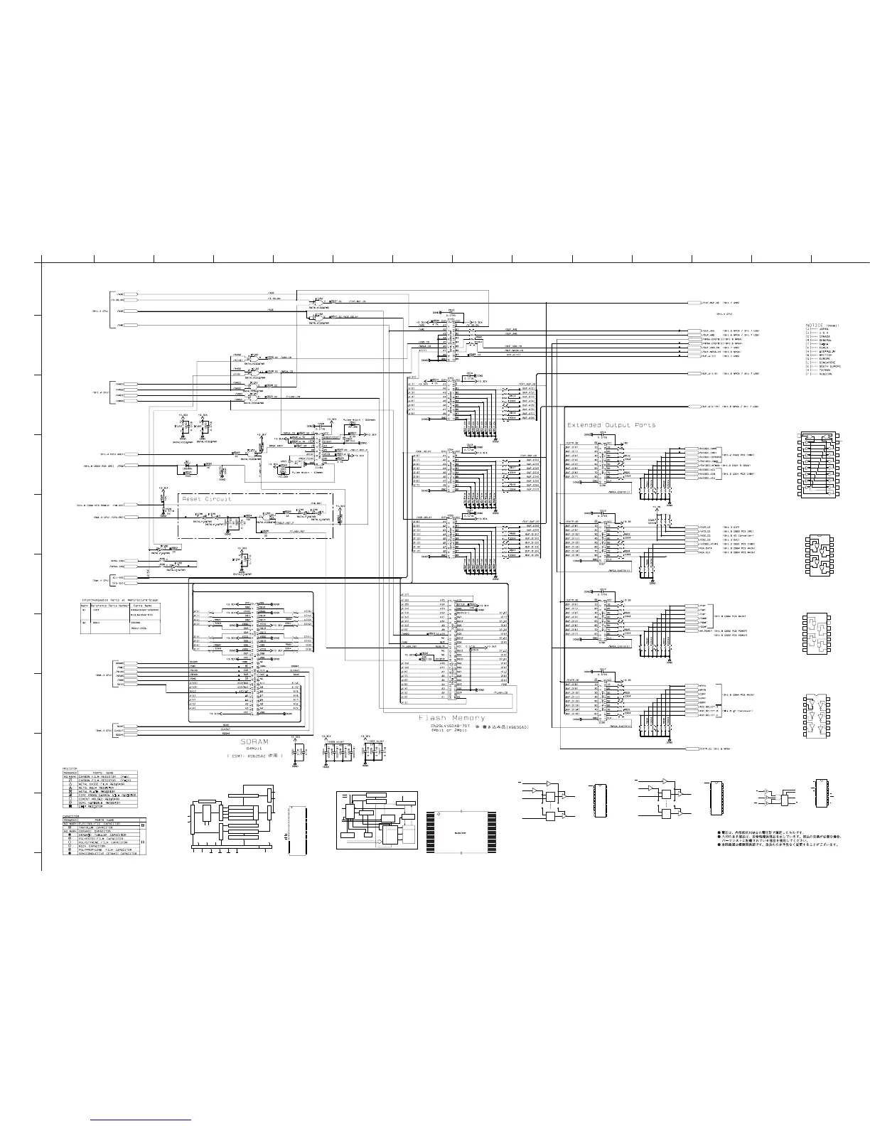
IC152
IC152
IC152
IC152
IC153
IC153
IC153
IC153
IC155IC155
IC155IC155
IC155
IC155
IC51
IC52
IC154
IC59
IC58
IC57
IC56
IC55
IC54
IC53
IC151
A
1
2
3
4
5
6
7
8
9
10
BCDEFGH I JK
L MN
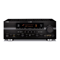
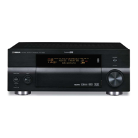
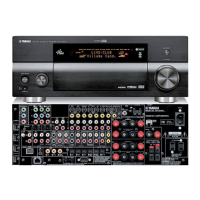
RX-V463/HTR-6140/DSP-AX463
89
★ All voltages are measured with a 10MΩ/V DC electronic voltmeter.
★ Components having special characteristics are marked s and must be replaced
with parts having specifications equal to those originally installed.
★ Schematic diagram is subject to change without notice.
DSP 5/8
3.2
3.2
0
3.2
3.3
3.3
3.2
3.3
3.0
3.2
3.3
3.3
3.3
3.3
3.3
3.3
3.3 3.3
3.3
3.3
00
3.3
3.3
00
3.3
3.3
3.3
3.3
3.3
3.2
3.3
3.3
0
0
0
3.3
3.3
3.3
0
3.3
1.3
3.3
3.3
3.2
0
3.3
0
3.3
0
3.2
3.3
1.1
3.01.1
3.3
3.3
1.3
3.3
0.4
0
0.4
0
3.3
0.4
0.4
0.4
0
0.3
0.5
3.3
0.3
0
0
1.7
3.3
0.6
0.4
1.2
3.3
0.4
3.1
1.8
0
0.6
1.3
1.1
1.2
0
0.9
3.3
0
0
1.0
0
3.3
3.3
3.3
3.3
1.1
2.2
3.3
3.3
3.3
3.3
3.3
3.3
3.3
0
0.13.3
3.3
3.3
3.3
3.3
0
0
3.2
3.2
0
0
0
0
3.3
3.3
3.3
3.3
0
3.2
3.3
3.3
3.3
3.3
3.3
1.8
3.1
0.4
3.3
0
0
0
0
0
0
0.2
0
0
3.2
3.3
3.2
1.3
1.3
0.6
1.2
1.1
0.9
1.0
0
0
0
0
0
0
0
0
0
0
3.2
3.3
3.2
0.3
0.5
0.3
0.4
0.4
0.4
0.4
0.4
0
0
0
3.3
0
0.4
0
0.4
0
1.0
0.4
0.9
0.4
1.1
3.3
0.4
1.2
0.3
0.6
0.5
1.3
0.3
1.3
3.3
0
3.3
3.3
1.3
1.9
1.2
1.4
1.3
3.3
3.3
3.3
3.3
3.3
0
0
3.1
1.8
3.3
0.4
3.3
3.3
0
0
0
0
0
0
0
0
0
5.0
5.0
0
0
0
0
0
0
0
0
0
0
0
0
4.9
0
3.3
0
3.3
4.9
0
3.3
0
0
0
0
0
0
0
0
0
0
3.3
3.0
3.3
0
0
0
3.3
0
3.3
3.3
0
0
0
0
0
0
0
0
0
0
3.3
3.3
3.3
3.3
3.3
0
3.3
0
3.3
3.3
0
0
0
0
0
0
0
0
0
0
0
3.3
0
3.3
1.8
3.1
3.3
0.3
IC51: K4S641632K-UC60000
64 M synchronous DRAM
Bank Select
CLK
Row Decoder
I/O Control
Output Buffer
Sense AMP
Address Register
Data Input Register
Column Decoder
Latency & Burst Length
Programming Register
2M x 8 / 1M x16
2M x 8 / 1M x16
2M x 8 / 1M x16
2M x 8 / 1M x16
Col. Buffer
Row Buffer
Refresh Counter
ADD
LCKE
LRAS
CLK
LRAS
LCAS
Timing Register
LCBR LWE
DQi
LDQM
LWE
LWCBR
CKE CS
LCBR
WE L(U)DQM
LDQM
RAS CAS
1
VDD
VDD
VSS
N.C/RFU
VSS
VSS
VSSQ
VSSQ
VDDQ
VDDQ
DQ15
A4
A5
A6
A7
A8
A9
A11
CKE
CLK
N.C
DQ14
DQ13
DQ12
DQ11
DQ10
DQ9
DQ8
UDQM
V
DDQ
VDDQ
VSSQ
VSSQ
DQ0
DQ1
DQ2
DQ3
DQ4
DQ5
DQ6
DQ7
2
3
4
5
6
7
8
9
10
11
12
13
14
15
16
17
18
19
20
21
22
23
24
25
26
27
30
29
28
33
32
31
36
35
34
39
38
41
40
43
42
45
44
46
48
47
50
49
51
53
54
52
37
BA0
LDQM
V
DD
WE
CAS
RAS
CS
BA1
A10/AP
A3
A0
A1
A2
IC155: SN74LV14APWR
Hex schmitt trigger inverters
GND
Y3
A3
A2
A1
VCC
A6
A5
A4
Y6
Y5
Y4
Y2
Y1
1
2
3
4
5
6
7
14
13
12
11
10
9
8
1
DIR
A1
A2
A3
A4
A5
A6
A7
A8
GND
Vcc
OE
B1
B2
B3
B4
B5
B6
B7
B8
2
3
4
5
6
7
8
9
10
20
19
18
17
16
15
14
13
12
11
IC53-55, 151: SN74LVC245APWR
Octal bus transceivers with 3-state outputs
4B13
4A12
4Y11
3B10
3A9
3Y8
1B 2
1Y 3
2A 4
2B 5
2Y 6
GND 7
IC152: SN74LVC32APW
Quadruple 2-input positive-OR gates
Vcc141A 1
1
2
3
4
5
6
7
8
9
10
20
19
18
17
16
15
14
13
12
11
OE
1D
2D
3D
4D
5D
6D
7D
8D
GND
V
CC
1Q
2Q
3Q
4Q
5Q
6Q
7Q
8Q
CLK
IC56: SN74AHCT574PWR
Octal edge-triggered D-type flip-flops with 3-state outputs
OE
1
11
2
19
CLK
1D
C1
1D
1Q
9
12
8D
C8
8D
8Q
1
2
3
4
5
6
7
8
9
10
20
19
18
17
16
15
14
13
12
11
OE
1D
2D
3D
4D
5D
6D
7D
8D
GND
V
CC
1Q
2Q
3Q
4Q
5Q
6Q
7Q
8Q
CLK
IC57-59: SN74LV574APWR 8D-F
Octal edge-triggered D-type flip-flops with 3-state outputs
OE
1
11
2
19
CLK
1D
C1
1D
1Q
9
12
8D
C8
8D
8Q
4B13
4A12
4Y11
3B10
3A9
3Y8
1B 2
1Y 3
2A 4
2B 5
2Y 6
GND 7
IC153: SN74LVC08APWR
Quadruple 2-input positive-AND gate
Vcc141A 1
IC154: SN74LV123APWR
Dual retriggerable monostable multivibrators with schmitt-trigger inputs
1B
1CLR
2CLR
1A
A
B
Q
Q
CLR
2B
2A
VCC
1Q
2Q
GND
1Q
2Q
2C
ext
2R
ext
/C
ext
R
ext
/C
ext
C
ext
1R
ext
/C
ext
1C
ext
2
3
4
5
6
7
8
1
15
14
13
12
11
10
9
16
R
IC52: EN29LV160AB-70TCP
16 M-bit flash memory boot sector flash memory, CMOS 3.0 V-only
Vcc Detector
Timer
Program Voltage
Generator
Chip Enable
Output Enable
Logic
Y-Decoder
Input/Output buffers
Y-G a t i n g
Cell Matrix
X-Decoder
Address Latch
Erase Voltage Generator
Block Protect Switches
WE#
CE#
OE#
A0-A19
Vcc
RY/BY#
Vss
DQ0-DQ15 (A-1)
STB
STB
State
Control
Command
Register
Data Latch
A1
A15
A18
A14
A13
A12
A11
A10
A19
A9
A8
NC
WE#
RESET#
NC
NC
RY/BY#
A17
A7
A6
A5
A4
A3
A2
1
16
2
3
4
5
6
7
8
17
18
19
20
21
22
23
24
9
10
11
12
13
14
15
A16
DQ2
BYTE#
V
SS
DQ15/A-1
DQ7
DQ14
DQ6
DQ13
DQ9
DQ1
DQ8
DQ0
OE#
V
SS
CE#
A0
DQ5
DQ12
DQ4
V
CC
DQ11
DQ3
DQ10
48
33
47
46
45
44
43
42
41
40
39
38
37
36
35
34
25
32
31
30
29
28
27
26
EXTENDED PORTS
SDRAM
BUS BUFFER
BUS BUFFER
FLASH MEMORY
to DSP 4/8
to DSP 4/8
to DSP 4/8
to DSP 4/8
to DSP 4/8
to DSP 4/8
to DSP 4/8
to DSP 8/8
to DSP 8/8
to DSP 7/8
to DSP 6/8 / to DSP 7/8
to DSP 6/8 / to DSP 7/8
to DSP 7/8
to DSP 7/8
to DSP 2/8
to DSP 2/8
to DSP 2/8
to DSP 2/8
to DSP 8/8
to DSP 8/8
to DSP 8/8
to DSP 8/8
to DSP 8/8
to DSP 8/8
to DSP 8/8
to DSP 6/8
to DSP 8/8
to DSP 8/8
to DSP 3/8
to DSP 3/8
to DSP 6/8
to DSP 6/8 / to DSP 7/8
to DSP 6/8 / to DSP 7/8
to DSP 6/8
to DSP 6/8
to DSP 4/8
 Loading...