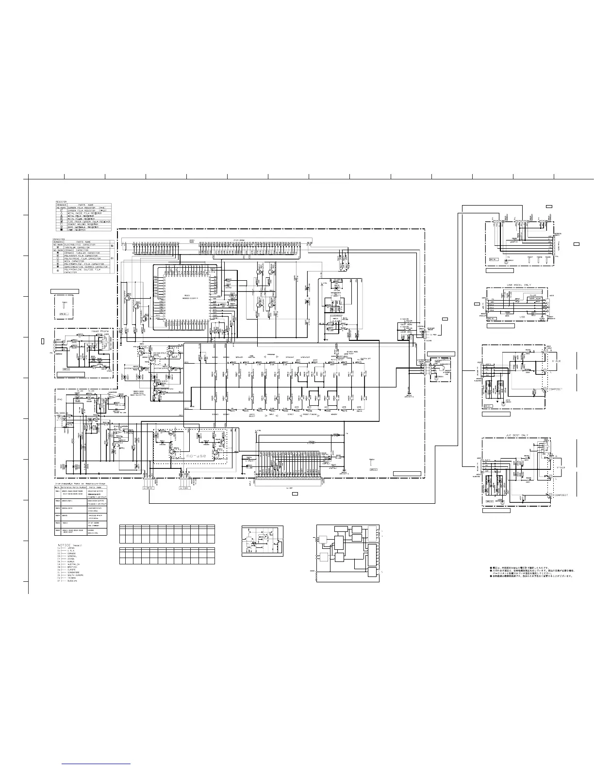
IC603
CB601
JK602
IC601
IC601
IC601
JK601
W6001
W6009
CB603
W6005
CB604
CB605 CB606W6004
W6008
W6007
JK603
W6006
CB607
CB610
CB609
CB608
CB602
A
1
2
3
4
5
6
7
8
9
10
BCDEFGH I JK
L MN
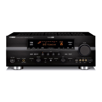
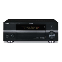
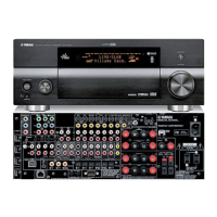
RX-V463/HTR-6140/DSP-AX463
93
★ All voltages are measured with a 10MΩ/V DC electronic voltmeter.
★ Components having special characteristics are marked s and must be replaced
with parts having specifications equal to those originally installed.
★ Schematic diagram is subject to change without notice.
OPERATION 1/2
-30.7
-30.7
-30.7
-30.7
-30.7
-30.7
-30.7
-30.7
-30.7
-30.7
-30.7
-30.7
-30.7
-30.7
3.3
1.5
1.5
0
0
3.2
3.2
3.3
-30.7
-30.7
-30.7
-30.7
-30.7
-30.7
-30.7
-30.7
-30.7
-30.7
-30.7
-29.0
3.3
-29.0
-29.0
3.3
-29.0
-29.0
3.3
-29.0
-30.7
-30.7
-30.7
-30.7
-30.7
-30.7
-30.7
-29.0
-29.0
-29.0
-29.1
-29.1
-29.1
-29.1
-29.1
-29.1
-29.1
-29.1
-29.1
-29.1
-29.1
-29.1
-29.1
-29.1
-30.9
-30.7
-30.7
-30.7
-30.7
-30.7
-30.7
-23.1
-23.1
-29.1
-29.1
-29.1
-29.1
-29.1
-29.1
-29.1
-29.1
-29.1
-29.1
-29.1
-29.1
-29.1
-29.1
-29.0
-29.0
-29.0
-30.7
-30.7
-30.7
-30.7
-30.7
-30.7
-30.7
-30.7
-30.7
-30.7
-30.7
-30.7
-30.7
-30.7
-30.6
-30.7
-30.6
-30.6
-30.7
-30.7
-30.7
-30.7
-30.7
-30.7
-30.7
-30.7
-30.7
-30.7
-30.7
-30.7
-30.7
-30.7
-30.7
-30.7
-2.3.1
-23.1
-30.7
-30.7
-30.6
3.3
-30.6
-30.7
3.3
-30.6
-30.7
3.3
-30.6
-30.7
3.3
-30.6
-30.7
3.3
0
0
0
3.3
3.3
3.3
0
2.0
2.0
2.0
2.0
0
0
3.3
0
1.3
5.1
0
0
0
-11.8
0
1.1
12.1
0
11.6
3.3
2.0
0.3
0
0
3.3
0
0
0
0
0
3.3
2.6
2.0
3.3
-30.9
3.3
0
3.3
-27.2
-27.2
-23.6
00
0
0
0
0
0
0
0
0
0
0
0
0
0
0
0
0
52
Display
controller
Serial
receive
circuit
Digit
output
circuit
Clock
generator
DIG11/
SEG42
51
DIG12/
SEG41
50
DIG13/
SEG40
49
DIG14/
SEG39
48
DIG15/
SEG38
47
DIG16/
SEG37
46
DIG17/
SEG36
45
SEG35
XOUT
6
Vcc1
8
Vcc2
18
Vss
5
Vp
64
XIN
7
CS
SCK
3
SDATA
4
RESET
1
SEG00
44
9
SEG34
SEG26
17
19
SEG25
Segment
output
circuit
Display code
RAM
(8-bit x 60)
CGROM
(35-bit x 166)
CGROM
(35-bit x 16)
code
select
Code
write
Code/
command
control
circuit
DIG00
63
53
DIG10
IC603: M66003-0131FP-R
18 digit 5 x 7 segment VFD controller/driver
2
data
timing
clock
dot data
write
scan pulse
Segment/
Digit
select/
output
circuit
IC601: NJM4565M
Dual operational amplifier
8
2, 6
3, 5
1, 7
4
V+
–INPUT
+INPUT
V–
OUTPUT
VFD
OPERATION (9)
OPERATION (3)
OPERATION (1)
OPERATION (7)
OPERATION (4)
OPERATION (6)
OPERATION (8)
OPERATION (5)
U, C, J models
R, T, K, A, B, G, E, F, L models
R, T, K, A, B, G, E, F, L models
USB
STANDBY/ON
PHONES
OPTIMIZER
MIC
VOLUME
AUDIO
VIDEO AUX
VIDEO
AUDIO
PORTABLE
VIDEO AUX
VIDEO
BAND
INFO
TUNING AUTO/MAN'L
to DSP_CB71
Page 91
K9
to DSP_CB83
Page 92
L3
to OPERATION (2)_CB703
Page 94
H8
to MAIN_W501
Page 95
I4
to MAIN_W401
Page 96
E3
to VIDEO (1)_W3001
Page 97
E2
Ohm
V
KEY
INPUT 0
(7 pin)
KEY
INPUT 1
(6 pin)
0
0–0.2
–
–
+ 1.0 k
0.2–0.4
SPEAKERS
A/B/OFF
–
+ 1.0 k
0.4–0.7
TONE
CONTROL
AUDIO
SELECT
+ 1.5 k
0.7–1.0
PROGRAM
<
INPUT
>
+ 2.2 k
1.0–1.3
PROGRAM
>
INPUT
<
+ 2.2 k
1.3–1.6
STRAIGTH
EFFECT
DIRECT
+ 3.3 k
1.6–1.9
A/B/C/D/E
PRESET/
TUNING
<
+ 4.7 k
1.9–2.1
BAND
PRESET/
TUNING
>
+ 6.8 k
2.1–2.4
MEMORY
+ 10.0 k
2.4–2.7
EDIT
PRESET/
TUNING
INFO
TUNING
AUTO/
MAN’L
Key detection for A/D port
Key input (A/D) pull-up resistance 10 k-ohms
U, C, R, T, K, A, G, E, F, L, J models
+ 22.0 k
2.7–3.0
Ohm
V
KEY
INPUT 0
(7 pin)
KEY
INPUT 1
(6 pin)
0
0–0.2
–
–
+ 1.0 k
0.2–0.4
SPEAKERS
A/B/OFF
–
+ 1.0 k
0.4–0.7
TONE
CONTROL
AUDIO
SELECT
+ 1.5 k
0.7–1.0
PROGRAM
<
INPUT
>
+ 2.2 k
1.1–1.3
PROGRAM
>
INPUT
<
+ 2.2 k
1.3–1.6
STRAIGTH
EFFECT
DIRECT
+ 3.3 k
1.6–1.9
–
–
+ 4.7 k
1.9–2.1
–
–
+ 6.8 k
2.1–2.4
–
–
–
+ 10.0 k
2.4–2.7
–
–
–
B model
+ 22.0 k
2.7–2.9
–
–
–
 Loading...