Do you have a question about the YouKits TJ2B and is the answer not in the manual?
Assemble the 2MHz crystal, bending leads before soldering.
Solder MIC GND pin to CN6 GND and MIC pin to MIC pad.
Modify and assemble the 3.5mm stereo socket to J1 for external MIC/PTT.
Solder a 220uF capacitor to C7 pads.
Solder a miniature transformer to T1 pads.
Insert LCD cable to FFC socket CN3, bending the flexible cable.
Fasten two 6mm brass stand-offs to mounting holes with screws.
Solder the four function buttons onto the DDS board.
Split end leads to fit CN1 and solder the 7-wire cable.
Push LCD window through frame, fasten with screws, and optionally use glue.
Solder the 5-pin socket to CN2 for encoder and tuning rate port.
Solder the MIC cable to CN5 using the yellow connector.
Assemble the SETUP switch on the PCB back.
Setup procedures for IFS and DDS clock value calibration.
Adjust USB/LSB frequency separation to 1.4 kHz.
Assemble two DC input sockets.
Assemble the power switch.
Assemble the PTT switch, but not the push button yet.
Assemble the 3.5mm stereo phone socket.
Assemble connectors CN3, CN4, CN5, CN6, CN7.
Assemble two TQ2 relays, noting PCB and relay bars.
Solder 220uF electrolytic capacitors to specified pads, observing polarity.
Solder the 9 MHz crystals onto the main board Y1-Y5 pads.
Solder can inductors (T4, L2, L3) to the main board.
Solder miniature transformers T1, T2, T3, T5, T6.
Assemble the 10k trimmer on CN2 pads, adjusting leads.
Assemble VC1 (variable capacitor), noting mounting direction.
Solder 10uF chip capacitor at C27, noting polarity.
Assemble inductors L1, L12, L13, L14, L15, including winding coils.
Assemble RFC4 (resistor) and RFC5 (inductor).
Assemble broadband transformer T7 on binocular core using bifilar turns.
Assemble broadband transformer T8 on FT37-43 core using bifilar turns.
Assemble the bias resistor R62 for the power transistor.
Assemble D18 on PCB back, parallel with a 100 ohm resistor.
Install a jump wire in JP3.
Jump JP1 and JP2 with hookup wire on PCB back.
Construct the power transistor assembly, bending leads, using insulator.
Solder 2-wire cable to speaker pads and assemble connector.
Mount the DDS Unit to the enclosure using pre-made stand-offs.
Position DDS Unit, ensuring fit, and tighten with stand-offs and washers.
Split screen braid of 50-ohm cable, tin leads, and solder.
Solder 3-wire cable to AF GAIN 10k pot, noting GND pin.
Connect ribbon and speaker cables to CN5 and CN6 respectively.
Connect the encoder.
Connect 12V DC to J3 or J2, observing polarity and switch position.
Measure BFO frequency at C40 test point and adjust L2/VC1 for target frequencies.
Adjust 10k trimmer on CN2 for maximum LED brightness.
Solder 50 ohm cable and connect MIC cable.
Connect antenna, set AF GAIN, and tune to 7MHz, adjust T4.
Align IF trap L3 by adjusting slug for weakest noise at 8.9900MHz.
Fasten encoder, AF GAIN pot, ANT socket to the top cover.
Slide main board into enclosure, aligning power switch handle.
Maneuver enclosure side wall to fit main board, then push main board in.
Cut ANT socket tail if too long to fit space, then fasten cover.
Solder ANT leads.
Assemble two brass stand-offs with tails to mounting holes.
Assemble power transistor assembly to main board, fastening aluminium.
Install the PTT button.
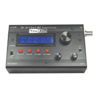
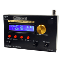
Overview of controls and connectors on the top cover.
Description of the BNC antenna socket.
Explanation of the MIC socket for external mic and PTT.
AF GAIN controls volume; turn clockwise to increase.
TUNE knob for frequency and tuning rate selection.
MOD button switches mode between LSB, USB, CW (RX).
A/B button selects VFO A/B or clears memories.
V/M button switches between VFO and memory modes.
MEM button saves frequency or transfers memory to VFO.
Controls for battery, power off, and external power selection.
Sockets for battery charging and earphones/speaker.
Details on bias resistor R62 (680 ohms).
Instructions for fitting the LCD holder, possibly modifying mounting holes.
Notes on BFO calibration, potential issues, and IF setting adjustments.
Advice on soldering the EXT PWR socket to ease main board insertion.
Step-by-step instructions for disassembling the transceiver for repair or improvement.
Identify DC cable center (+) and outer (-) wires, advising Ohm meter confirmation.
Lists differences in components for Kit B compared to Kit A.
Schematic block diagram of the TJ2B transceiver.
Calibrate L3 by tuning frequency to 8.998000MHz and adjusting for weakest noise.
Addresses low receive sound issue, suggesting cold solder joints or broken SMD caps.
Details identifying and testing broken SMD caps (C1, C2, C5, C14) for signal issues.
Guide to calibrating DDS clock and BFO using a frequency counter.
Select the correct channel (CH1) and gate time (1s, 10MHz) on the frequency counter.
Procedure to calibrate DDS clock using a frequency counter and IFS setting.
Connect frequency counter to BFO test point and adjust L2/VC1 for target frequencies.
Troubleshooting VC1 adjustment issues related to frequency counter or crystal variation.
Addresses BFO frequency drift, explaining the need for warming-up time.
Verify clock calibration at highest band frequency (18.199999MHz).
Emphasizes frequency counter accuracy for DDS/BFO calibration.
| Brand | YouKits |
|---|---|
| Model | TJ2B |
| Category | Transceiver |
| Language | English |