- 47 -
Feed-back Circuit
C817
27P J
R819
3M
D805
BAV99
A
J
K
C838
4700P J
C837
0.033U K
R825
422 F
R827
422 F
C815
3.3N J
CN801
2062204102
1
1
2
2
C814
5P D
D809
BAV99
A
J
K
R820
3.3K F
C819
0.22U M
D806
BAV99
A
J
K
C846
0.01U K
F1
F2
R823
100K
.
.
.
T801
1J.26049.031
1
8
6
7
4
3
C816
27P J
TP801
TP802
Fig. 9
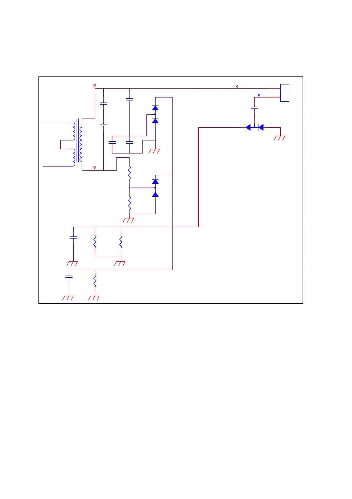
Fig. 2 shows the feedback circuit consists of a lamp, C846, D809, R825, R827 and C837.
With the lamp current through D809, a half sin-waveform voltage signal is produced. We
may get the Maximum value through R825/R827/C837.
After OZ9938 gets the feedback voltage signal from PIN5, the duty of the PWM driver
outputs is decided.

 Loading...