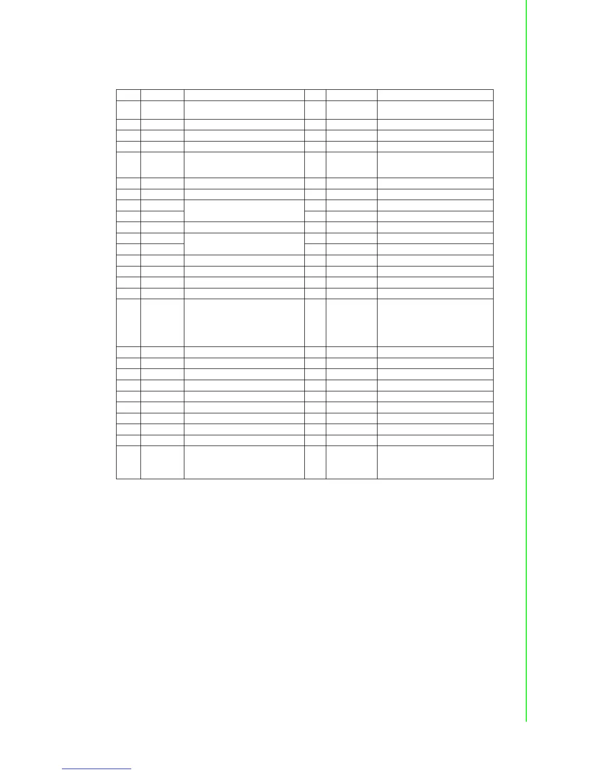
Pin Assignments
A.8 Mini PCIE Slot (MINI PCIE)
Supports PCI 1.1 and 1.2 power definition.
* +3.3 V aux was suspend power with power out to device +3.3 V/1.1A
* +3.3 V was core power
* +1.5 V was core power with power out to device +1.5 V/0.5A
Pin Signal Description Pin Signal Description
52
+3.3 V aux/
+3.3 V
PCI 1.1 was +3.3 V, PCI 1.2 was +3.3 V
aux
51 Reserved NC
50 GND 49 Reserved NC
48 +1.5 V 47 Reserved NC
46 NC NC 45 Reserved NC
44 NC NC 43
PIN43_MPCIE_
PWRSEL
Pin for selecting Pin 2; 52 power output
for +3.3 V aux or +3.3 V (PCI 1.1 was
reserved and PIC1.2 was GND)
42 NC NC 41 +3.3Vaux
40 GND 39 +3.3Vaux
38 USB_D+
USB serial data interface compliant to
the USB 2.0 specification
37 GND
36 USB_D- 35 GND
34 GND 33 PETp0 PCI Express differential transmit pair
32 SMB_DATA
SMBus data signal compliant to SMBus
2.0 specification
31 PETn0
30 SMB_CLK 29 GND
28 +1.5 V 27 GND
26 GND 25 PERp0 PCI Express differential receive pair
24 +3.3 V aux 23 PERn0
22 PERST# Functional reset to the card 21 GND
20
W_DISABLE
#
Active low signal. This signal is used by
the system to disable radio operation on
add-in cards that implement radio fre-
quency applications. When implemented,
this signal requires a pull-up resistor on
the card.
19 Reserved NC
18 GND 17 Reserved NC
Key Key Key Key
16 NC NC 15 GND
14 NC NC 13 REFCLK+
12 NC NC 11 REFCLK-
10 NC NC 9 GND
8 NC NC 7 CLKREQ# Reference clock request signal
6 1.5 V 5 NC NC
4GND 3NC NC
2
+3.3 V aux/
+3.3 V
PCI 1.1 was +3.3 V, PCI 1.2 was +3.3 V
aux
1 WAKE#
Open drain active low signal. This sig-
nal is used to request that the system
return from a sleep/suspended state to
service a function-initiated wake event.