92 Principles of Operation
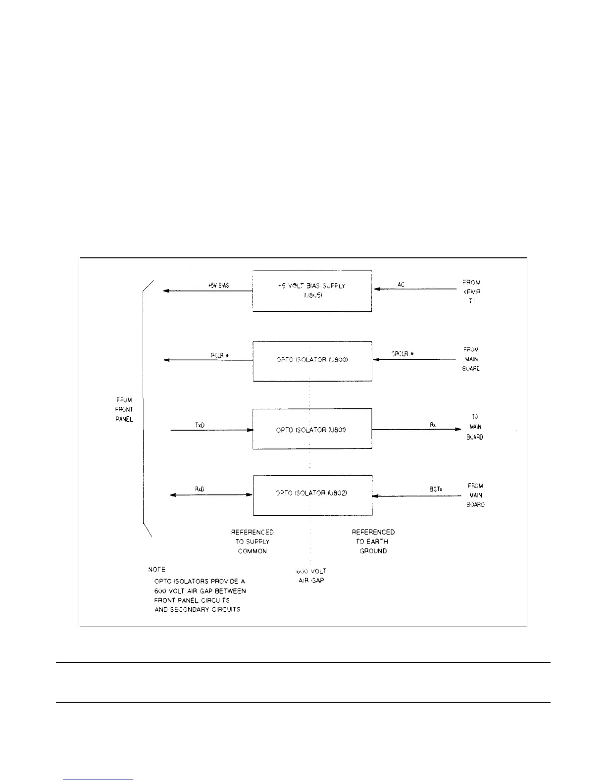
When power is turned on to the power supply, an isolated AC signal from XFMR T1 in the secondary circuits is applied to a
+5 V bias supply (U805) on the isolator board. The bias supply produces a +5 V BIAS output voltage that is routed to the
front panel circuits.
At the same time, a low SPCLR* level from the secondary circuits is applied to optical isolator circuit, U800. It is then
routed as a low PCLR* level to the RESET* input of the front panel microprocessor. This low level keeps the
microprocessor temporarily disabled during power turn-on for a short time interval.
After a time delay of 40 ms, SPCLR* goes high and the microprocessor is enabled. By inhibiting microprocessor operation
for 40 ms, any erroneous operation (due to a rising but yet unstable +5 V) is prevented until the +5 V BIAS voltage fully
settles.
When power is turned off or is removed, SPCLR* goes low immediately and disables the microprocessor in order to
provide a graceful shut down of the power supply as the +5 V falls to zero volts. See Figure 4-8 which shows the time delay
of the *PCLR signal, which is obtained from the isolated *SPCLR signal.
Figure 4-7. Isolator Board, Simplified Block Diagram (Models Agilent 654xA and 655xA)
Note Note that for Agilent 664xA and 665xA models, the PCLR* is generated in the GPIB board. For Agilent
models 654xA and 655xA, the PCLR* originates at the main board secondary circuits and is routed to the
isolator board.
 Loading...