21 / 31
ZYNQ FPGA Development Platform AC7015 User Manual
Amazon Store: https://www.amazon.com/alinx
Sales Email: rachel.zhou@aithtech.com
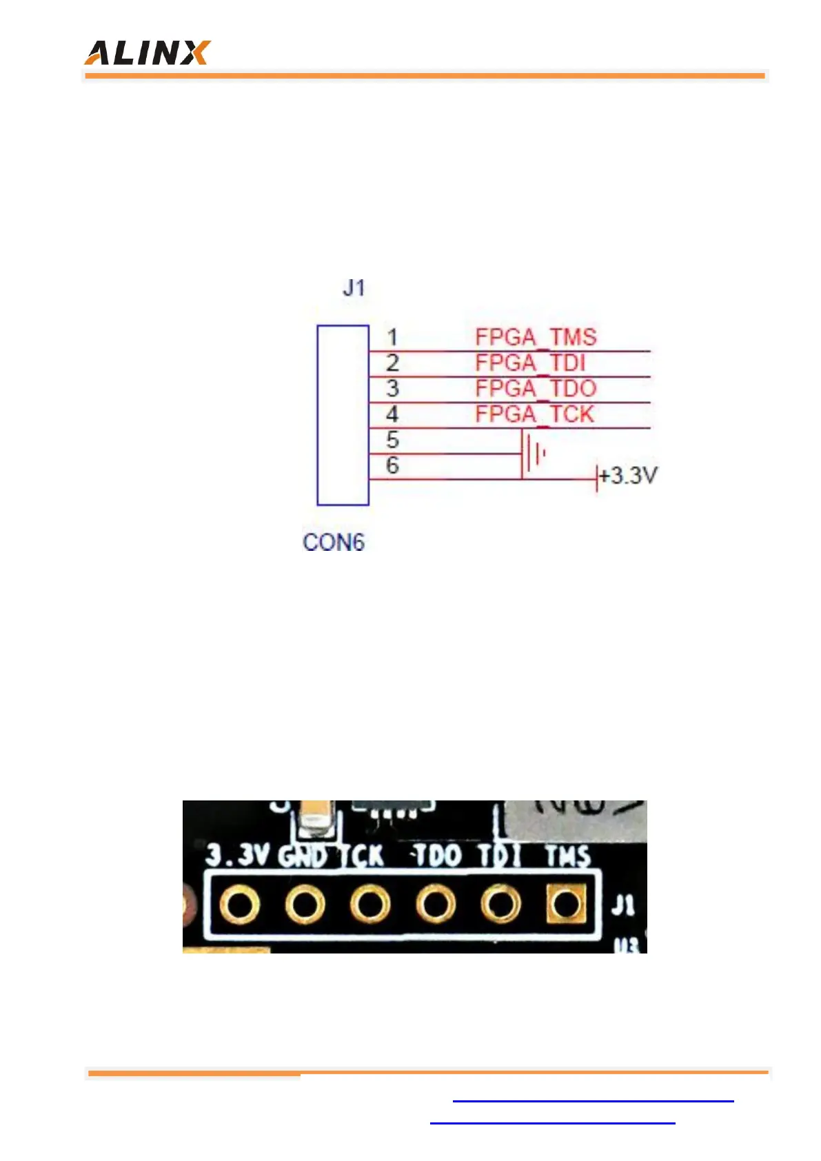
Part 10: JTAG Interface
The JTAG test socket J1 is reserved on the AC7015 core board for separate
JTAG download and debugging of the core board. Figure 2-10-1 is the schematic
part of the JTAG port, which involves TMS, TDI, TDO, TCK, GND. , +3.3V these
six signals.
Figure 10-1: JTAG interface part of the core board schematic
The JTAG interface J1 on the core board uses a 6-pin 2.54mm pitch single-
row test hole. If you need to use the JTAG connection to debug on the core board,
you need to solder a 6-pin single-row pin header. Figure 10-2 shows the physical
map of the JTAG interface on the development board.
Figure 10-2: JTAG interface on the core board