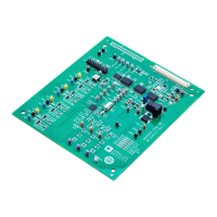
ADE9000 Technical Reference Manual UG-1098
Rev. 0 | Page 67 of 86
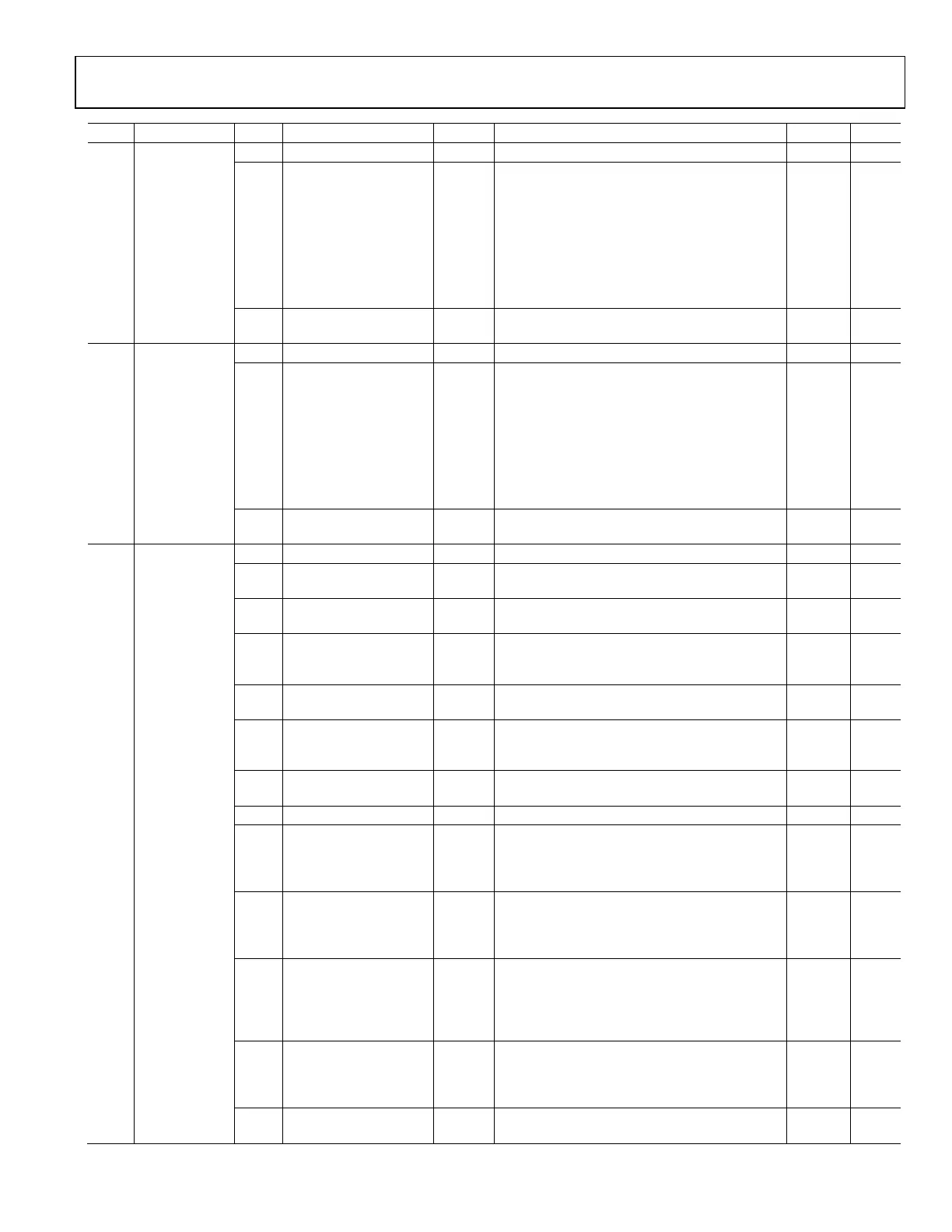
Addr. Name Bits Bit Name Settings Description Reset Access
0x400 IPEAK [31:27] RESERVED Reserved. 0x0 R
[26:24] IPPHASE These bits indicate which phases generate the
IPEAKVAL value. Note that the PEAKSEL, Bits[4:2]
in the CONFIG3 register determine which current
channel to monitor the peak value on. When
IPPHASE, Bit 0 is set to 1, Phase A current is
generated by the IPEAKVAL, Bits[23:0] value.
Similarly, IPPHASE, Bit 1 indicates that the Phase B
and IPPHASE, Bit 2 indicates that the Phase C
current generated the peak value.
0x0 R
[23:0] IPEAKVAL The IPEAK register stores the absolute value of
the peak current. IPEAK is equal to xI_PCF/2
5
.
0x0 R
0x401 VPEAK [31:27] RESERVED Reserved. 0x0 R
These bits indicate which phase(s) generate the
VPEAKVAL value. Note that the PEAKSEL,
Bits[4:2] in the CONFIG3 register determine which
voltage channels to monitor the peak value on.
When VPPHASE, Bit 0 is 1, the Phase A voltage
generated the VPEAKVAL, Bits[23:0] value.
Similarly, VPPHASE, Bit 1 indicates Phase B and
VPPHASE, Bit 2 indicates that the Phase C
voltage generated the peak value.
[23:0] VPEAKVAL The VPEAK register stores the absolute value of
the peak voltage. VPEAK is equal to xV_PCF/2
5
.
0x0 R
0x402 STATUS0 [31:26] RESERVED Reserved. 0x0 R
This bit goes high to indicate when a new
temperature measurement is available.
24 MISMTCH This bit is set to indicate a change in the
relationship between ISUMRMS and ISUMLVL.
0x0 R/W1
23 COH_WFB_FULL This bit is set when the waveform buffer is full
with resampled data, which is selected when
WF_CAP_SEL = 0 in the WFB_CFG register.
0x0 R/W1
This bit is set when one of the events configured
in WFB_TRIG_CFG occurs.
21 THD_PF_RDY This bit goes high to indicate when the THD and
power factor measurements update, every
1.024 sec.
0x0 R/W1
20 RMS1012RDY
This bit is set when the 10 cycle rms/12 cycle rms
values update.
0x0 R/W1
This bit is set when the fast RMS½ values update.
18 PWRRDY This bit is set when the power values in the
xWATT_ACC, xVA_ACC, xVAR_ACC, xFWATT_ACC,
xFVA_ACC, and xFVAR_ACC registers update,
after PWR_TIME 8 kSPS samples.
0x0 R/W1
17 PAGE_FULL This bit is set when a page enabled in the
WFB_PG_IRQEN register is filled with fixed data
rate samples, when WF_CAP_SEL bit in the
WFB_CFG register is equal to zero.
0x0 R/W1
16 WFB_TRIG_IRQ This bit is set when the waveform buffer stops
filling after an event configured in WFB_TRIG_CFG
occurs. This happens with fixed data rate samples
only, when WF_CAP_SEL bit in the WFB_CFG
register is equal to zero.
0x0 R/W1
15 DREADY This bit is set when new waveform samples are
ready. The update rate depends on the data
selected in the WF_SRC bits in the WFB_CFG
register.
0x0 R/W1
14 CF4 This bit is set when a CF4 pulse is issued, when
the CF4 pin goes from a high to low state.
0x0 R/W1

 Loading...