ADE9000 Technical Reference Manual UG-1098
Rev. 0 | Page 79 of 86
Addr. Name Bits Bit Name Settings Description Reset Access
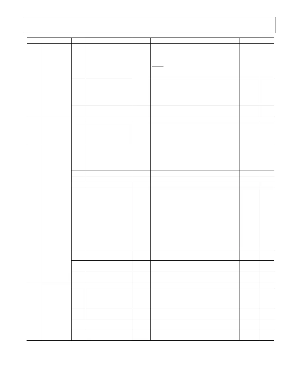
These bits select which function to output on
the CF4 pin.
00 CF4, from digital to frequency converter.
01 CF4, from digital to frequency converter.
10
EVENT
.
11 DREADY.
1 CF3_CFG This bit selects which function to output on the
CF3 pin.
0x0 R/W
0 CF3, from digital to frequency converter.
1 Zero-crossing output selected by the ZX_SEL bits
in the ZX_LP_SEL register.
0 SWRST Set this bit to initiate a software reset. Note that
this bit is self clearing.
0x0 W1
0x48F OISTATUS [15:4] RESERVED Reserved. 0x0 R
[3:0] OIPHASE OIPHASE, Bit 0 indicates Phase A is above OILVL. 0x0 R
OIPHASE, Bit 1 indicates Phase B is above OILVL.
OIPHASE, Bit 2 indicates Phase C is above OILVL.
OIPHASE, Bit 3 indicates Phase N is above OILVL.
0x490 CFMODE 15 CF4DIS CF4 output disable. Set this bit to disable the
CF4 output and bring the pin high. Note that
when this bit is set, the CFx bit in STATUS0 is not
set when a CF pulse is accumulated in the digital
to frequency converter.
0x0 R/W
14 CF3DIS CF3 output disable. See CF4DIS. 0x0 R/W
CF2 output disable. See CF4DIS.
12 CF1DIS CF1 output disable. See CF4DIS 0x0 R/W
[11:9] CF4SEL
Type of energy output on the CF4 pin. Configure
TERMSEL4 in the COMPMODE register to select
which phases are included.
0x0 R/W
000 Total active power.
001 Total reactive power.
010 Total apparent power.
Fundamental active power.
100 Fundamental reactive power.
101 Fundamental apparent power.
110 Total active power.
111 Total active power.
[8:6] CF3SEL Selects type of energy output on CF3 pin. See
CF4SEL.
0x0 R/W
[5:3] CF2SEL Selects type of energy output on CF2 pin. See
CF4SEL.
0x0 R/W
[2:0] CF1SEL Selects type of energy output on CF1 pin. See
CF4SEL.
0x0 R/W
[11:9] TERMSEL4 Phases to include in CF4 pulse output. Set
TERMSEL4, Bit 2 to 1 to include Phase C in the
CF4 pulse output. Similarly, set TERMSEL4, Bit 1 to
include Phase B, and TERMSEL4, Bit 0 for Phase A.
0x0 R/W
[8:6] TERMSEL3 Phases to include in CF3 pulse output. See
TERMSEL4.
0x0 R/W
Phases to include in CF2 pulse output. See
TERMSEL4.
[2:0] TERMSEL1 Phases to include in CF1 pulse output. See
TERMSEL4.
0x0 R/W

 Loading...