EasyManua.ls Logo

Atmel AT90S2313 User Manual

Atmel AT90S2313
87 pages
To Next Page IconTo Next Page
To Previous Page IconTo Previous Page
Page #40 background imageLoading...
Page #40 background image
AT90S2313
40
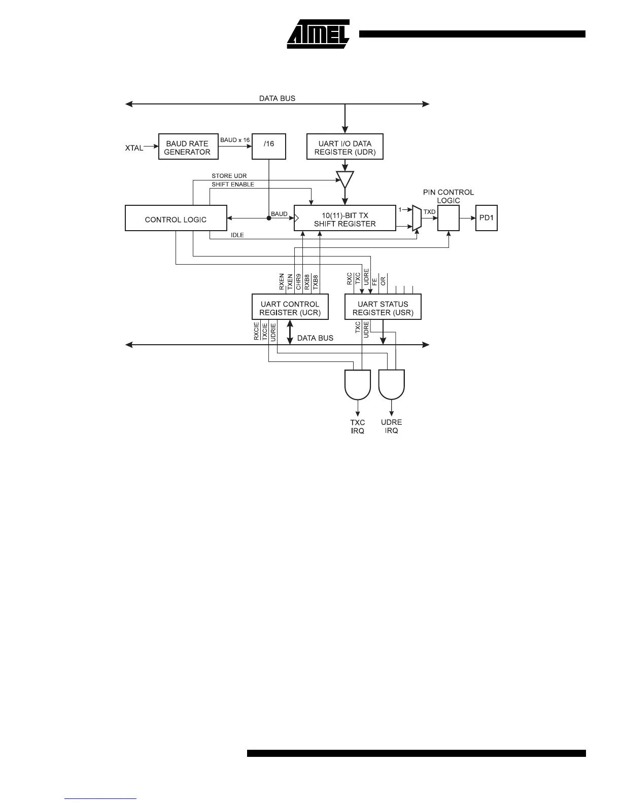
Figure 34. UART Transmitter
If the 10(11)-bit Transmitter shift register is empty, data is transferred from UDR to the shift register. At this time the UDRE
(UART Data Register Empty) bit in the UART Status Register, USR, is set. When this bit is set (one), the UART is ready to
receive the next character. At the same time as the data is transferred from UDR to the 10(11)-bit shift register, bit 0 of the
shift register is cleared (start bit) and bit 9 or 10 is set (stop bit). If 9 bit data word is selected (the CHR9 bit in the UART
Control Register, UCR is set), the TXB8 bit in UCR is transferred to bit 9 in the Transmit shift register.
On the Baud Rate clock following the transfer operation to the shift register, the start bit is shifted out on the TXD pin. Then
follows the data, LSB first. When the stop bit has been shifted out, the shift register is loaded if any new data has been
written to the UDR during the transmission. During loading, UDRE is set. If there is no new data in the UDR register to send
when the stop bit is shifted out, the UDRE flag will remain set until UDR is written again. When no new data has been
written, and the stop bit has been present on TXD for one bit length, the TX Complete Flag, TXC, in USR is set.
The TXEN bit in UCR enables the UART transmitter when set (one). When this bit is cleared (zero), the PD1 pin can be
used for general I/O. When TXEN is set, the UART Transmitter will be connected to PD1, which is forced to be an output
pin regardless of the setting of the DDD1 bit in DDRD.
Question and Answer IconNeed help?

Do you have a question about the Atmel AT90S2313 and is the answer not in the manual?

Atmel AT90S2313 Specifications

General IconGeneral
ArchitectureAVR
Flash Memory2 KB
SRAM128 bytes
EEPROM128 bytes
I/O Pins15
ADCNo
Timers1 x 8-bit, 1 x 16-bit
Data Bus Width8-bit
Instruction Set ArchitectureRISC
ManufacturerAtmel
CoreAVR
PackageSOIC

Summary

Features of AT90S2313 Microcontroller

AVR RISC Architecture

High-performance, low-power RISC architecture with single clock cycle execution.

Memory Features

2K Flash, 128B SRAM, 128B EEPROM with endurance specifications.

Peripheral Features

Includes timers, PWM, comparator, Watchdog, SPI, and UART modules.

Pin Configuration

Pin Descriptions

Architectural Overview

General Purpose Register File

In-System Programmable Flash Program Memory

EEPROM Data Memory

SRAM Data Memory Organization

Program and Data Addressing Modes

Memory Access and Instruction Execution Timing

I/O Memory Map

Status Register - SREG

Reset and Interrupt Handling

Reset Sources

Power-On Reset

External Reset

Watchdog Reset

Interrupt Handling

External Interrupts

MCU Control Register - MCUCR

Sleep Modes

Power Down Mode

Oscillator stopped; wake-up via external reset or interrupt.

Timer/Counters Overview

8-bit Timer/Counter0

Timer/Counter0 Control Register - TCCR0

16-bit Timer/Counter1

Timer/Counter1 Control Register A - TCCR1A

Timer/Counter1 Control Register B - TCCR1B

Timer/Counter1 - TCNT1H and TCNT1L

Timer/Counter1 Output Compare Register A

Timer/Counter1 Input Capture Register

Timer/Counter1 in PWM Mode

Watchdog Timer Functionality

Watchdog Timer Control Register - WDTCR

EEPROM Read/Write Access

EEPROM Control Register - EECR

Prevent EEPROM Corruption

UART Overview

UART Data Reception

UART Control

UART Control Register - UCR

Baud Rate Generator Functionality

Analog Comparator Overview

Analog Comparator Control and Status Register - ACSR

Analog Comparator Control Bits

Port B Description

Alternate Functions of Port B

Port D Description

Alternate Functions of Port D

Memory Programming Overview

Fuse Bits Configuration

Programming the Flash and EEPROM

Parallel Programming Interface

Enter Programming Mode

Chip Erase Procedure

Programming the Flash Memory

Reading the Flash Memory

Programming the EEPROM Memory

Reading the EEPROM Memory

Programming the Fuse Bits

Programming the Lock Bits

Parallel Programming Characteristics

Serial Downloading Procedure

Serial Programming Algorithm

Serial Programming Characteristics

Electrical Characteristics

Absolute Maximum Ratings

Operating limits to prevent device damage.

DC Characteristics

Register Summary

Instruction Set Summary

Instruction Set Summary (Continued)

Related product manuals