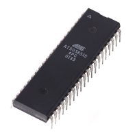
AT90S2313
39
Caution: An interrupt between step 4 and step 5 will make the write cycle fail, since the EEPROM Master Write Enable will
time-out. If an interrupt routine accessing the EEPROM is interrupting another EEPROM access, the EEAR or EEDR regis-
ter will be modified, causing the interrupted EEPROM access to fail. It is recommended to have the global interrupt flag
cleared during the 4 last steps to avoid these problems.
•
Bit 0 - EERE: EEPROM Read Enable
The EEPROM Read Enable Signal EERE is the read strobe to the EEPROM. When the correct address is set up in the
EEAR register, the EERE bit must be set. When the EERE bit is cleared (zero) by hardware, requested data is found in the
EEDR register. The EEPROM read access takes one instruction and there is no need to poll the EERE bit. When EERE
has been set, the CPU is halted for two cycles before the next instruction is executed.
The user should poll the EEWE bit before starting the read operation. If a write operation is in progress when new data or
address is written to the EEPROM I/O registers, the write operation will be interrupted, and the result is undefined.
Prevent EEPROM Corruption
During periods of low V
CC,
the EEPROM data can be corrupted because the supply voltage is too low for the CPU and the
EEPROM to operate properly. These issues are the same as for board level systems using the EEPROM, and the same
design solutions should be applied.
An EEPROM data corruption can be caused by two situations when the voltage is too low. First, a regular write sequence
to the EEPROM requires a minimum voltage to operate correctly. Secondly, the CPU itself can execute instructions incor-
rectly, if the supply voltage for executing instructions is too low.
EEPROM data corruption can easily be avoided by following these design recommendations (one is sufficient):
1. Keep the AVR RESET active (low) during periods of insufficient power supply voltage. This is best done by an
external low V
CC
Reset Protection circuit, often referred to as a Brown-Out Detector (BOD). Please refer to applica-
tion note AVR 180 for design considerations regarding power-on reset and low voltage detection.
2. Keep the AVR core in Power Down Sleep Mode during periods of low V
CC
. This will prevent the CPU from attempt-
ing to decode and execute instructions, effectively protecting the EEPROM registers from unintentional writes.
3. Store constants in Flash memory if the ability to change memory contents from software is not required. Flash
memory can not be updated by the CPU, and will not be subject to corruption.
UART
The AT90S2313 features a full duplex (separate receive and transmit registers) Universal Asynchronous Receiver and
Transmitter (UART). The main features are:
• Baud rate generator that can generate a large number of baud rates (bps)
• High baud rates at low XTAL frequencies
• 8 or 9 bits data
• Noise filtering
• Overrun detection
• Framing Error detection
• False Start Bit detection
• Three separate interrupts on TX Complete, TX Data Register Empty and RX Complete
Data Transmission
A block schematic of the UART transmitter is shown in Figure 34.
Data transmission is initiated by writing the data to be transmitted to the UART I/O Data Register, UDR. Data is transferred
from UDR to the Transmit shift register when:
• A new character has been written to UDR after the stop bit from the previous character has been shifted out. The shift
register is loaded immediately.
• A new character has been written to UDR before the stop bit from the previous character has been shifted out. The shift
register is loaded when the stop bit of the character currently being transmitted has been shifted out.
 Loading...
