AT90S2313
42
When the stop bit enters the receiver, the majority of the three samples must be one to accept the stop bit. If two or more
samples are logical zeros, the Framing Error (FE) flag in the UART Status Register (USR) is set. Before reading the UDR
register, the user should always check the FE bit to detect Framing Errors.
Whether or not a valid stop bit is detected at the end of a character reception cycle, the data is transferred to UDR and the
RXC flag in USR is set. UDR is in fact two physically separate registers, one for transmitted data and one for received data.
When UDR is read, the Receive Data register is accessed, and when UDR is written, the Transmit Data register is
accessed. If 9 bit data word is selected (the CHR9 bit in the UART Control Register, UCR is set), the RXB8 bit in UCR is
loaded with bit 9 in the Transmit shift register when data is transferred to UDR.
If, after having received a character, the UDR register has not been read since the last receive, the OverRun (OR) flag in
UCR is set. This means that the last data byte shifted into to the shift register could not be transferred to UDR and has been
lost. The OR bit is buffered, and is updated when the valid data byte in UDR is read. Thus, the user should always check
the OR bit after reading the UDR register in order to detect any overruns if the baud rate is high or CPU load is high.
When the RXEN bit in the UCR register is cleared (zero), the receiver is disabled. This means that the PD0 pin can be used
as a general I/O pin. When RXEN is set, the UART Receiver will be connected to PD0, which is forced to be an input pin
regardless of the setting of the DDD0 bit in DDRD. When PD0 is forced to input by the UART, the PORTD0 bit can still be
used to control the pull-up resistor on the pin.
When the CHR9 bit in the UCR register is set, transmitted and received characters are 9-bit long plus start and stop bits.
The 9th data bit to be transmitted is the TXB8 bit in UCR register. This bit must be set to the wanted value before a trans-
mission is initiated by writing to the UDR register. The 9th data bit received is the RXB8 bit in the UCR register.
UART Control
The UART I/O Data Register - UDR
The UDR register is actually two physically separate registers sharing the same I/O address. When writing to the register,
the UART Transmit Data register is written. When reading from UDR, the UART Receive Data register is read.
UART Status Register - USR
The USR register is a read-only register providing information on the UART Status.
•
Bit 7 - RXC: UART Receive Complete
This bit is set (one) when a received character is transferred from the Receiver Shift register to UDR. The bit is set regard-
less of any detected framing errors. When the RXCIE bit in UCR is set, the UART Receive Complete interrupt will be
executed when RXC is set(one). RXC is cleared by reading UDR. When interrupt-driven data reception is used, the UART
Receive Complete Interrupt routine must read UDR in order to clear RXC, otherwise a new interrupt will occur once the
interrupt routine terminates.
•
Bit 6 - TXC: UART Transmit Complete
This bit is set (one) when the entire character (including the stop bit) in the Transmit Shift register has been shifted out and
no new data has been written to UDR. This flag is especially useful in half-duplex communications interfaces, where a
transmitting application must enter receive mode and free the communications bus immediately after completing the
transmission.
When the TXCIE bit in UCR is set, setting of TXC causes the UART Transmit Complete interrupt to be executed. TXC is
cleared by hardware when executing the corresponding interrupt handling vector. Alternatively, the TXC bit is cleared
(zero) by writing a logical one to the bit.
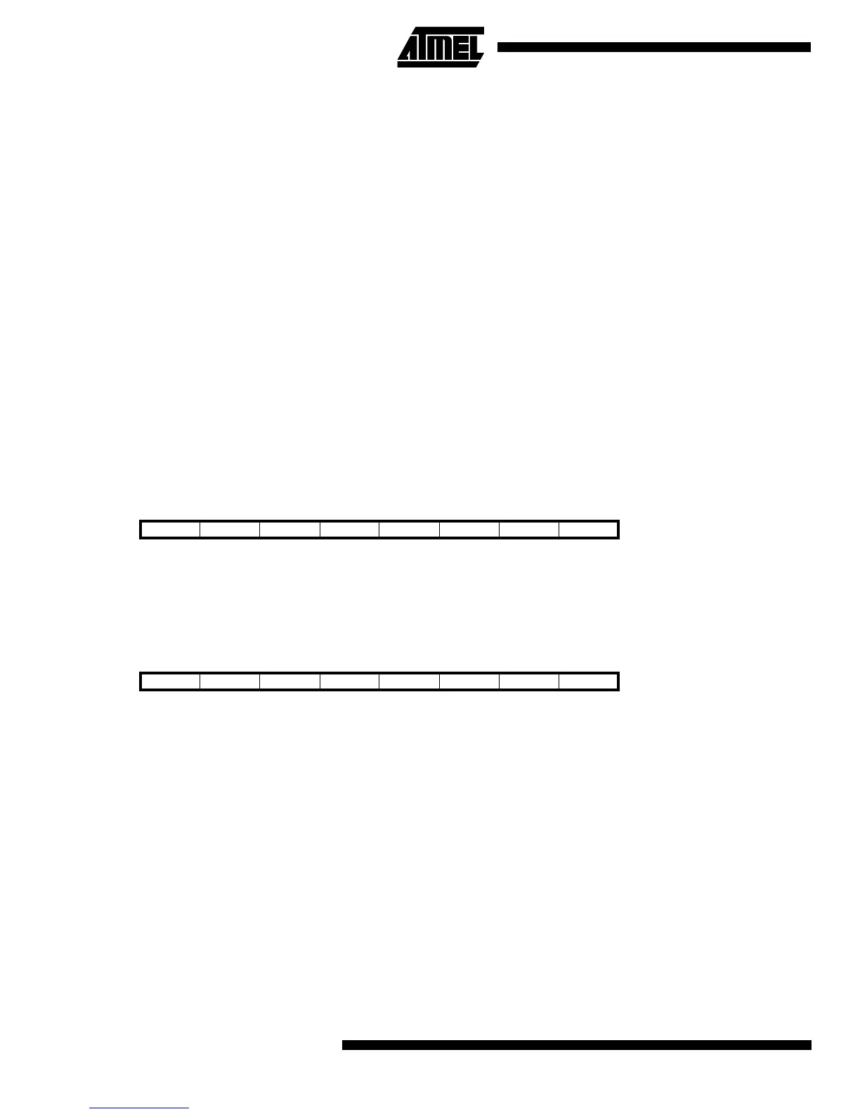
Bit 76543210
$0C ($2C) MSB LSB UDR
Read/Write R/W R/W R/W R/W R/W R/W R/W R/W
Initial value 0 0 0 0 0 0 0 0
Bit 76543210
$0B ($2B) RXC TXC UDRE FE OR - - - USR
Read/Write R R/W R R R R R R
Initial value 0 0 1 0 0 0 0 0