AT90S2313
68
Serial Programming Characteristics
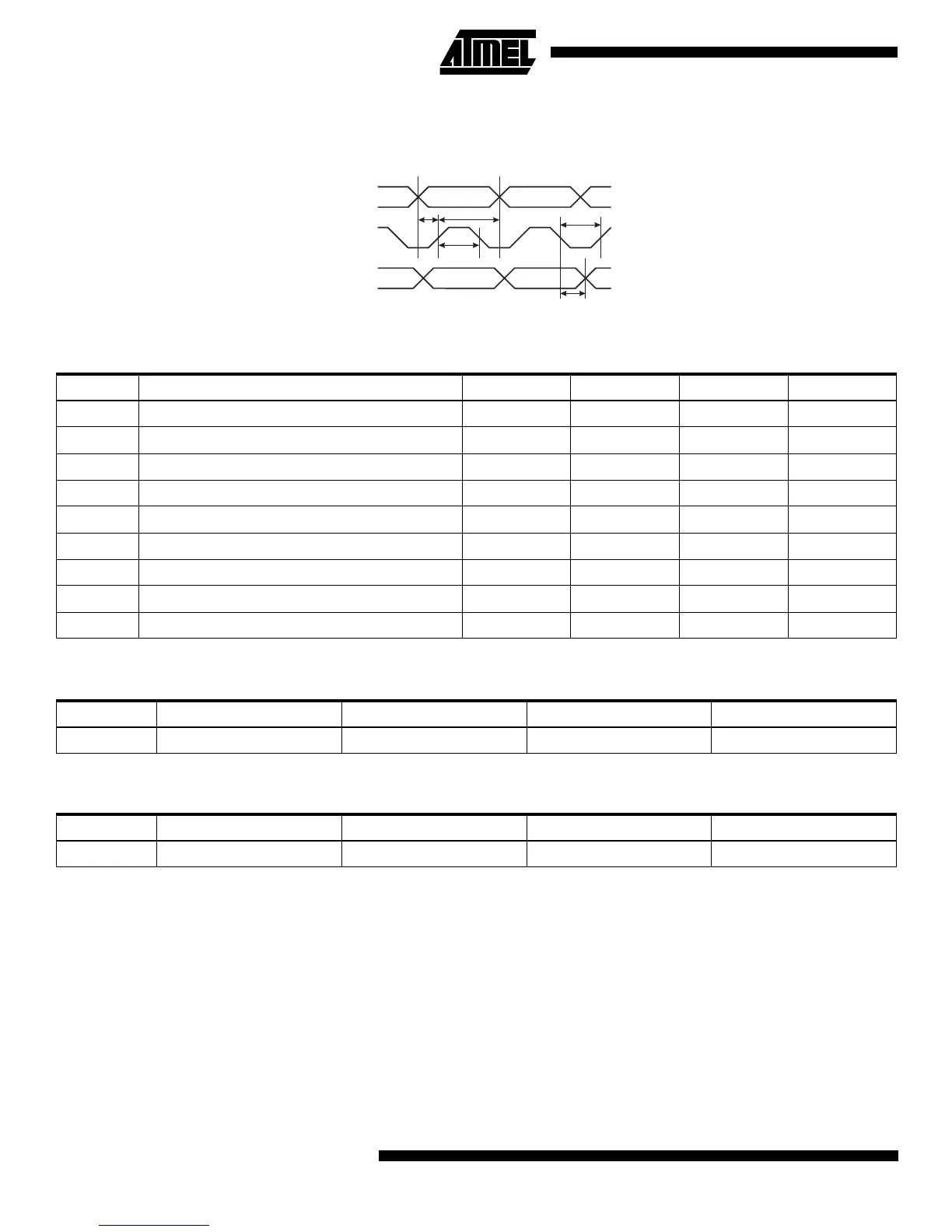
Figure 55. Serial Programming Timing
Table 29. Serial Programming Characteristics
T
A
= -40°C to 85°C, V
CC
= 2.7 - 6.0V (Unless otherwise noted)
Symbol Parameter Min Typ Max Units
1/t
CLCL
Oscillator Frequency (V
CC
= 2.7 - 6.0V) 0 4 MHz
t
CLCL
Oscillator Period (V
CC
= 2.7 - 6.0V) 250 ns
1/t
CLCL
Oscillator Frequency (V
CC
= 4.0 - 6.0V) 0 8 MHz
t
CLCL
Oscillator Period (V
CC
= 4.0 - 6.0V) 125 ns
t
SHSL
SCK Pulse Width High 2 t
CLCL
ns
t
SLSH
SCK Pulse Width Low 2 t
CLCL
ns
t
OVSH
MOSI Setup to SCK High t
CLCL
ns
t
SHOX
MOSI Hold after SCK High 2 t
CLCL
ns
t
SLIV
SCK Low to MISO Valid 10 16 32 ns
Table 30. Minimum wait delay after the Chip Erase instruction
Symbol 3.2V 3.6V 4.0V 5.0V
t
WD_ERASE
18 ms 14 ms 12 ms 8 ms
Table 31. Minimum wait delay after writing a Flash or EEPROM location
Symbol 3.2V 3.6V 4.0V 5.0V
t
WD_PROG
9 ms 7 ms 6 ms 4 ms
MOSI
MISO
SCK
t
OVSH
t
SHSL
t
SLSH
t
SHOX
t
SLIV