AT90S2313
65
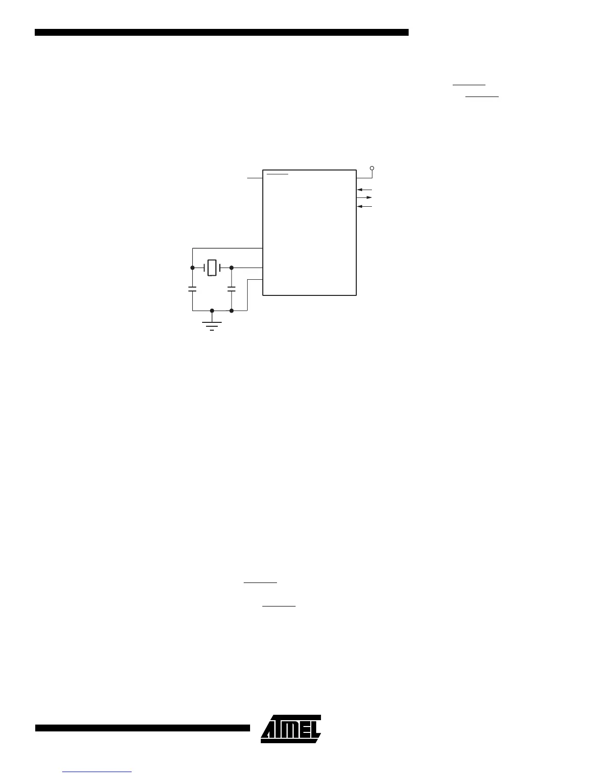
Serial Downloading
Both the Program and Data memory arrays can be programmed using the serial SPI bus while RESET is pulled to GND.
The serial interface consists of pins SCK, MOSI (input) and MISO (output), see Figure 53. After RESET
is set low, the
Programming Enable instruction needs to be executed first before program/erase instructions can be executed.
Figure 53. Serial Programming and Verify
For the EEPROM, an auto-erase cycle is provided within the self-timed write instruction and there is no need to first
execute the Chip Erase instruction. The Chip Erase instruction turns the content of every memory location in both the
Program and EEPROM arrays into $FF.
The Program and EEPROM memory arrays have separate address spaces, $0000 to $03FF for Program Flash memory
and $000 to $07F for EEPROM Data memory.
Either an external clock is supplied at pin XTAL1 or a crystal needs to be connected across pins XTAL1 and XTAL2. The
minimum low and high periods for the serial clock (SCK) input are defined as follows:
Low: > 2 XTAL1 clock cycle
High: > 2 XTAL1 clock cycles
Serial Programming Algorithm
When writing serial data to the AT90S2313, data is clocked on the rising edge of SCK.
When reading data from the AT90S2313, data is clocked on the falling edge of SCK. See Figure 54, Figure 55 and Table
29 for timing details.
To program and verify the AT90S2313 in the serial programming mode, the following sequence is recommended (See four
byte instruction formats in Table 28
):
1. Power-up sequence:
Apply power between V
CC
and GND while RESET and SCK are set to ‘0’. If a crystal is not connected across pins
XTAL1 and XTAL2, apply a clock signal to the XTAL1 pin. In some systems, the programmer can not guarantee that
SCK is held low during power-up. In this case, RESET
must be given a positive pulse of at least two XTAL1 cycles
duration after SCK has been set to ‘0’.
2. Wait for at least 20 ms and enable serial programming by sending the Programming Enable serial instruction to the
MOSI (PB5) pin.
AT90S2313
VCC
2.7 - 6.0V
PB7(SCK)
PB6(MISO)
PB5(MOSI)
RESET
GND
XTAL1
XTAL2
1 to 10 MHz
CLOCK IN
DATA OUT
INSTR. IN
GND