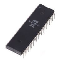
AT90S2313
66
3. The serial programming instructions will not work if the communication is out of synchronization. When in sync, the
second byte ($53) will echo back when issuing the third byte of the Programming Enable instruction. Whether the
echo is correct or not, all 4 bytes of the instruction must be transmitted. If the $53 did not echo back, give SCK a
positive pulse and issue a new Programming Enable instruction. If the $53 is not seen within 32 attempts, there is
no functional device connected.
4. If a Chip Erase is performed (must be done to erase the Flash), wait t
WD_ERASE
after the instruction, give RESET a
positive pulse, and start over from Step 2. See Table 30 on page 68 for t
WD_ERASE
value.
5. The Flash or EEPROM array is programmed one byte at a time by supplying the address and data together with the
appropriate Write instruction. An EEPROM memory location is first automatically erased before new data is written.
Use Data Polling to detect when the next byte in the Flash or EEPROM can be written. If polling is not used, wait
t
WD_PROG
before transmitting the next instruction. See Table 31 on page 68 for t
WD_PROG
value. In an erased device,
no $FFs in the data file(s) needs to be programmed.
6. Any memory location can be verified by using the Read instruction which returns the content at the selected
address at the serial output MISO (PB6) pin.
7. At the end of the programming session, RESET
can be set high to commence normal operation.
8. Power-off sequence (if needed):
Set XTAL1 to ‘0’ (if a crystal is not used).
Set RESET
to ‘1’.
Turn V
CC
power of
Data Polling EEPROM
When a byte is being programmed into the EEPROM, reading the address location being programmed will give the value
P1 until the auto-erase is finished, and then the value P2. See Table 27 for P1 and P2 values.
At the time the device is ready for a new EEPROM byte, the programmed value will read correctly. This is used to deter-
mine when the next byte can be written. This will not work for the values P1 and P2, so when programming these values,
the user will have to wait for at least the prescribed time
t
WD_PROG
before programming the next byte. See Table 30 for
t
WD_PROG
value. As a chip-erased device contains $FF in all locations, programming of addresses that are meant to contain
$FF, can be skipped. This does not apply if the EEPROM is reprogrammed without first chip-erasing the device.
Data Polling Flash
When a byte is being programmed into the Flash, reading the address location being programmed will give the value $7F.
At the time the device is ready for a new byte, the programmed value will read correctly. This is used to determine when the
next byte can be written. This will not work for the value $7F, so when programming this value, the user will have to wait for
at least t
WD_PROG
before programming the next byte. As a chip-erased device contains $FF in all locations, programming of
addresses that are meant to contain $FF, can be skipped.
Figure 54. Serial Programming Waveforms
Table 27. Read back value during EEPROM polling
Part P1 P2
AT90S2313 $80 $7F
