AT90S2313
27
•
Bits 1, 0 - ISC01, ISC00: Interrupt Sense Control 0 bit 1 and bit 0
The External Interrupt 0 is activated by the external pin INT0 if the SREG I-flag and the corresponding interrupt mask is set.
The level and edges on the external INT0 pin that activate the interrupt are defined in the following Table 6:
Note: When changing the ISC01/ISC00 bits, INT0 must be disabled by clearing its Interrupt Enable bit in the GIMSK Register. Other-
wise an interrupt can occur when the bits are changed.
The value on the INTn pin is sampled before detecting edges. If edge interrupt is selected, pulses with a duration longer
than one CPU clock period will generate an interrupt. Shorter pulses are not guaranteed to generate an interrupt. If low
level interrupt is selected, the low level must be held until the completion of the currently executing instruction to generate
an interrupt. If enabled, a level triggered interrupt will generate an interrupt request as long as the pin is held low.
Sleep Modes
To enter the sleep modes, the SE bit in MCUCR must be set (one) and a SLEEP instruction must be executed. If an
enabled interrupt occurs while the MCU is in a sleep mode, the MCU awakes, executes the interrupt routine, and resumes
execution from the instruction following SLEEP. The contents of the register file, SRAM and I/O memory are unaltered. If a
reset occurs during sleep mode, the MCU wakes up and executes from the Reset vector.
Idle Mode
When the SM bit is cleared (zero), the SLEEP instruction forces the MCU into the Idle Mode stopping the CPU but allowing
Timer/Counters, Watchdog and the interrupt system to continue operating. This enables the MCU to wake up from external
triggered interrupts as well as internal ones like Timer Overflow interrupt and watchdog reset. If wakeup from the Analog
Comparator interrupt is not required, the analog comparator can be powered down by setting the ACD-bit in the Analog
Comparator Control and Status register - ACSR. This will reduce power consumption in Idle Mode.
When the MCU wakes
up from Idle mode, the CPU starts program execution immediately.
Power Down Mode
When the SM bit is set (one), the SLEEP instruction forces the MCU into the Power Down Mode. In this mode, the external
oscillator is stopped
, while the external interrupts and the Watchdog (if enabled) continue operating. Only an external reset,
a watchdog reset (if enabled), an external level interrupt on INT0 or INT1 can wake up the MCU.
Note that when a level triggered interrupt is used for wake-up from power down, the low level must be held for a time longer
than the reset delay time-out period t
TOUT
. Otherwise, the device will not wake up.
Timer/Counters
The AT90S2313 provides two general purpose Timer/Counters - one 8-bit T/C and one 16-bit T/C. The Timer/Counters
have individual prescaling selection from the same 10-bit prescaling timer. Both Timer/Counters can either be used as a
timer with an internal clock timebase or as a counter with an external pin connection which triggers the counting.
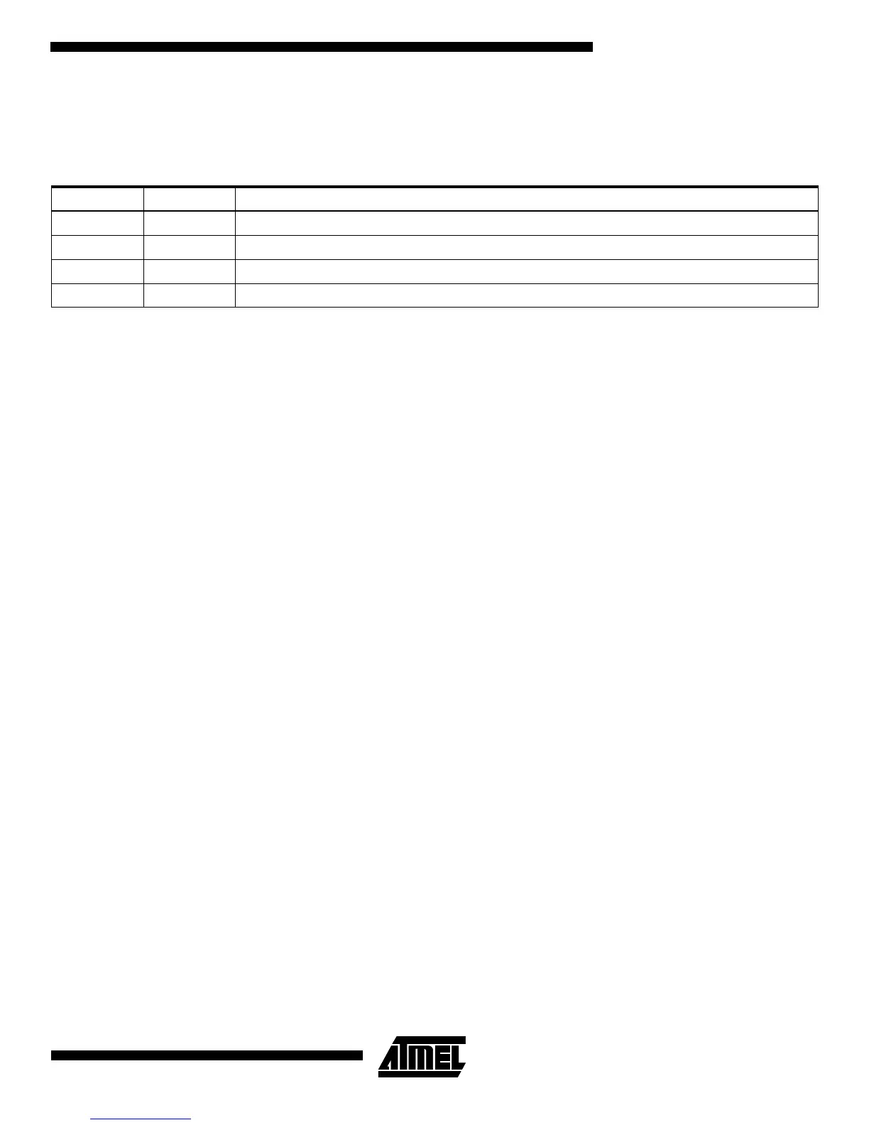
Table 6. Interrupt 0 Sense Control
ISC01 ISC00 Description
0 0 The low level of INT0 generates an interrupt request.
01Reserved
1 0 The falling edge of INT0 generates an interrupt request.
1 1 The rising edge of INT0 generates an interrupt request.