AT90S2313
56
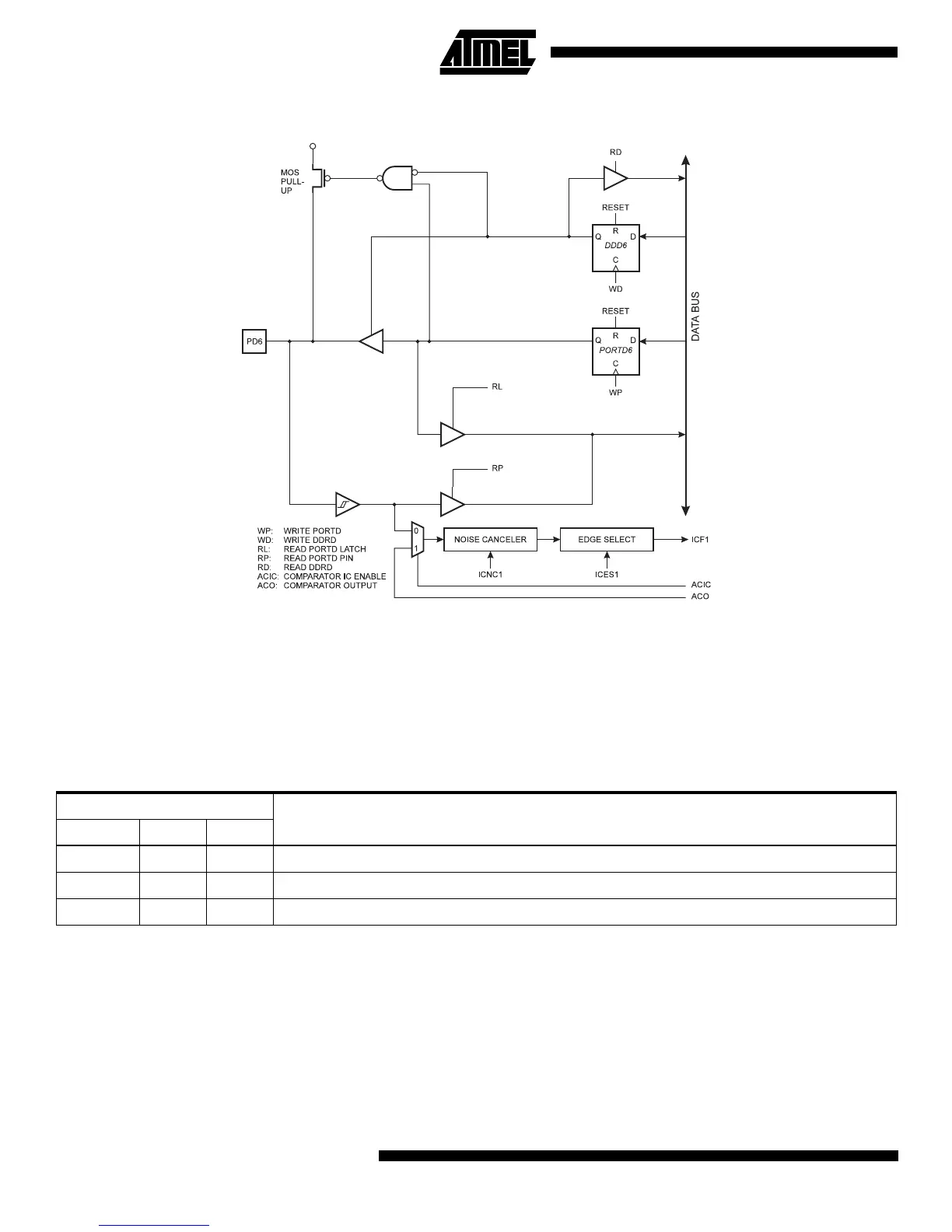
Figure 48. Port D Schematic Diagram (Pin PD6)
Memory Programming
Program and Data Memory Lock Bits
The AT90S2313 MCU provides two Lock bits which can be left unprogrammed (‘1’) or can be programmed (‘0’) to obtain
the additional features listed in Table 21
.
The Lock bits can only be erased with the Chip Erase operation.
Note: 1. In the Parallel mode, further programming of the Fuse bits are also disabled. Program the Fuse bits before programming the
Lock bits.
Table 21. Lock Bit Protection Modes
Memory Lock Bits
Protection TypeMode LB1 LB2
1 1 1 No memory lock features enabled.
2 0 1 Further programming of the Flash and EEPROM is disabled.
(1)
3 0 0 Same as mode 2, and verify is also disabled.